Diamond AFM Probes
For some AFM applications, such as nanoindentation or nanolithography a very hard and durable AFM tip is required. Some conductive AFM applications even require an extremely hard and at the same time conductive AFM tip. In such cases, AFM probes with metal coatings are not the right choice and the use of a diamond or even conductive diamond coated AFM probe is advised.
Diamond is the hardest material on earth. Like graphite, it consists of carbon but is considerably harder. The difference to graphite is the amount of (strong) sp3 atom-to-atom bindings instead of (weaker) sp2 bindings. In nature, the transition of carbon or graphite to diamond takes place under high pressure and high temperatures in the interior of the earth. To manufacture a diamond coated AFM probe, a carbon containing gas is being lead at high temperatures over a silicon AFM probe. If the process conditions are chosen the right way, the carbon will crystallize on the silicon surface and form a diamond layer. Usually diamond is growing in small (nano) crystallites. To form a close (and conductive) diamond layer, normally a diamond thickness of some 100 nm is required. This will result in a larger overall tip radius in the range of about some 100 nm for all diamond coated AFM probes. This is usually called the “macroscopic” tip radius. However, very often a single crystallite protrudes at the very end of the tip and thereby forms a small "extra-tip" with a radius in the 10 nm regime.

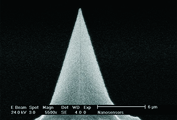
NANOSENSORS™ Diamond coated PointProbe tip.

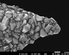
Diamond nano-crystallites are covering the very end of the silicon tip apex.

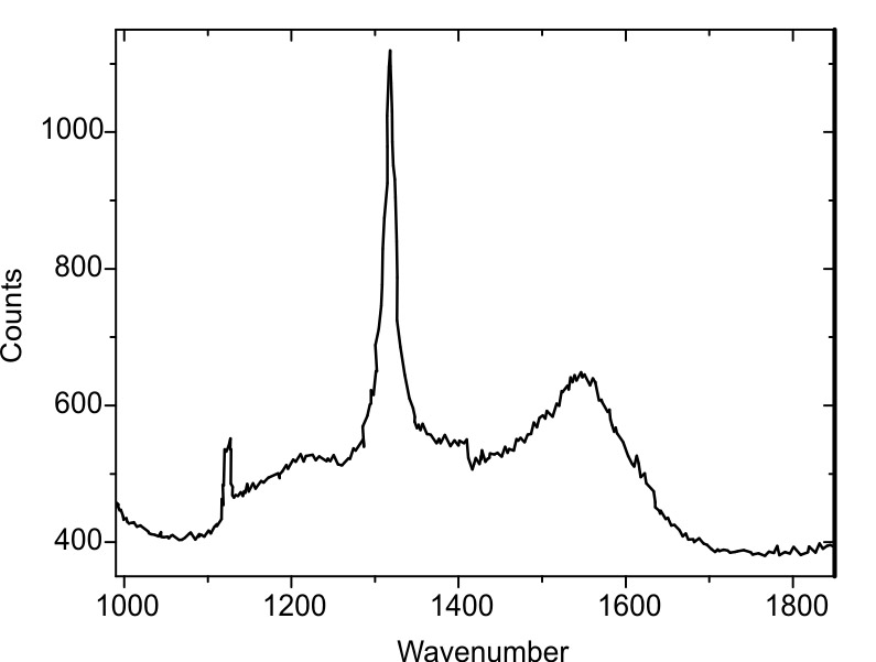
Raman spectrum of the diamond coating.
Unfortunately, pure diamond is not conductive. By adding other atoms with one electron less or more than carbon (so-called dopants) to the carbon gas, those atoms will be incorporated in the diamond crystallites during the growth process, thus enabling an electronic current flow. But unfortunately, the higher the number of dopants is, the lower the number of strong diamond sp3-bindings will be. As a result of the doping atom incorporation the diamond is getting softer. Here, a trade-off between hardness and conductivity has to be found.
The conductivity of doped diamond is – depending on the dopant atom concentration – roughly ten to hundred times less than for metals. But out of all conductive AFM probes, diamond – the hardest material on earth - is showing by far the smallest amount of wear.

Tip Shape: Standard


Tip Shape: Standard


Tip Shape: Standard


Tip Shape: Standard


Tip Shape: Standard


Tip Shape: Standard


Tip Shape: Standard


Diamond Coated, Conductive Force Modulation AFM Probe
Tip Shape: Standard


Tip Shape: Standard


Diamond Coated, Conductive Tapping Mode AFM Probe
Tip Shape: Standard


Diamond Coated, Conductive Force Modulation AFM Probe
Tip Shape: Standard


Tip Shape: Rotated


Tip Shape: various


Tip Shape: Standard


Tip Shape: Standard


Tip Shape: Standard


Diamond Coated, Conductive Tapping Mode AFM Probe
Tip Shape: Standard


Diamond Coated, Conductive Tapping Mode AFM Probe with Long Cantilever
Tip Shape: Standard


Tip Shape: Rotated

Tip Shape: various


