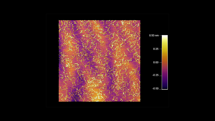
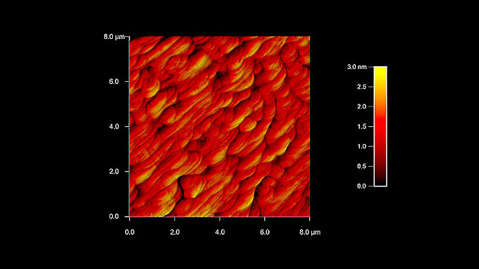
Topography image of dried DNA
Scanned with a BudgetSensors Tap300Al-G AFM probe on an Asylum Cypher AFM system, 5 micron scan size
Image courtesy of Scott MacLaren, University of Illinois at Urbana-Champaign, USA
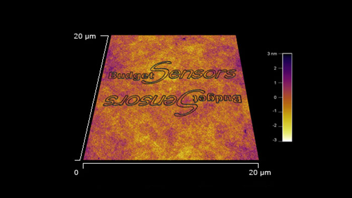
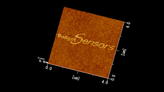
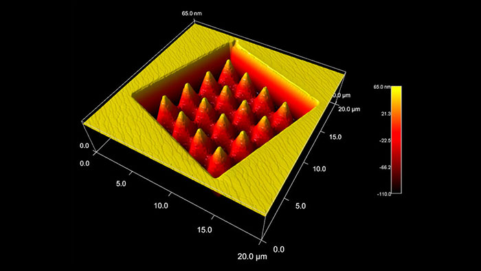
The BudgetSensors logo imprinted by scratch lithography on a flame annealed polycarbonate surface with a BudgetSensors Tap300Al-G AFM probe and an Asylum MFP 3D AFM system
Scanned with a BudgetSensors Tap300Al-G AFM probe on an Asylum MFP 3D AFM system, 20 micron scan size
Image courtesy of Scott MacLaren, University of Illinois at Urbana-Champaign, USA
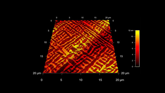
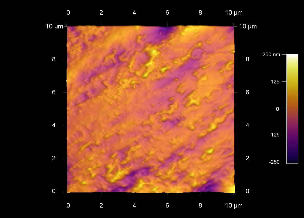
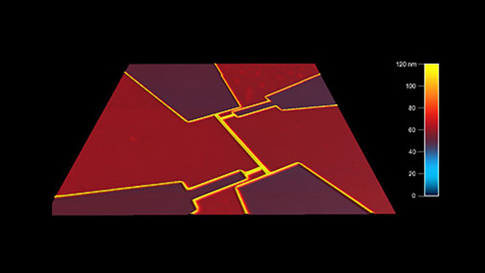
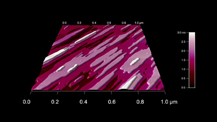
Bismuth iron oxide (BFO) thin film on lanthanum aluminate (LAO)
Scanned with a BudgetSensors Tap300Al-G AFM probe on an Asylum Cypher AFM system, 20 micron scan size
Image courtesy of Scott MacLaren, University of Illinois at Urbana-Champaign, USA
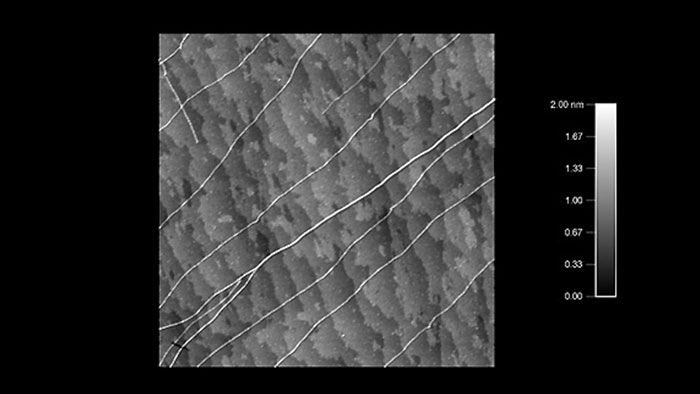
Scanned with a BudgetSensors Tap300Al-G AFM probe on an Asylum Cypher AFM system, 4 micron scan size
Image courtesy of Scott MacLaren, University of Illinois at Urbana-Champaign, USA
Scanned with a BudgetSensors Tap300Al-G AFM probe and an Asylum MFP 3D AFM system, 2 micron scan size
Image courtesy of Scott MacLaren, University of Illinois at Urbana-Champaign, USA
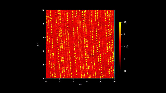
Scanned with a BudgetSensors Tap300Al-G AFM probe, 10 micron scan
Image courtesy of Scott MacLaren, University of Illinois at Urbana-Champaign, USA
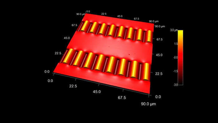
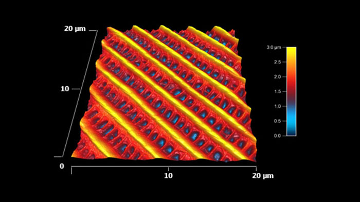
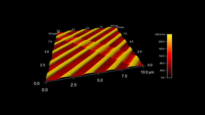
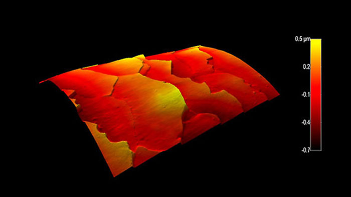
Compressed silicon nanoribbons on a flexible PDMS substrate
Scanned with a BudgetSensors Tap300Al-G AFM probe on an Asylum MFP-3D AFM system, 90 micron scan size
Image courtesy of Scott MacLaren, University of Illinois at Urbana-Champaign, USA
Magnetic field MFM image of a zip disk
Scanned with a BudgetSensors Multi75M-G AFM probe on an Asylum MFP-3D AFM system, 75 micron scan size
Image courtesy of Scott MacLaren, University of Illinois at Urbana-Champaign, USA
A superconducting quantum photon detecting device
Scanned with a BudgetSensors Tap300Al-G AFM probe on an Asylum MFP-3D AFM system, 25 micron scan size
Image courtesy of Scott MacLaren, University of Illinois at Urbana-Champaign, USA
Mouse skeletal muscle fiber
Scanned with a BudgetSensors Tap300Al-G AFM probe on an Asylum MFP-3D AFM system, 20 micron scan size
Image courtesy of Scott MacLaren, University of Illinois at Urbana-Champaign, USA
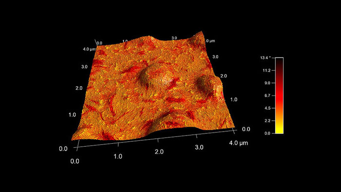
A screw dislocation in a polymer surface
Scanned with a BudgetSensors Tap300Al-G AFM probe on an Asylum MFP-3D AFM system, 3 micron scan size
Image courtesy of Scott MacLaren, University of Illinois at Urbana-Champaign, USA
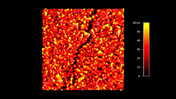
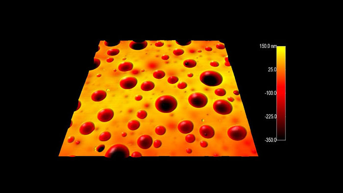
A crack in a nitride thin film
Scanned with a BudgetSensors Tap300Al-G AFM probe on an Asylum Cypher AFM system, 2 micron scan size
Image courtesy of Scott MacLaren, University of Illinois at Urbana-Champaign, USA
A gypsum crystal etched with water
Scanned with a BudgetSensors Tap300Al-G AFM probe on an Asylum Cypher AFM system, 3 micron scan size
Image courtesy of Scott MacLaren, University of Illinois at Urbana-Champaign, USA
Carbon nanotubes and bundles on quartz atomic steps
Scanned with a BudgetSensors Tap300Al-G AFM probe on an Asylum Cypher AFM system, 3 micron scan size
Image courtesy of Scott MacLaren, University of Illinois at Urbana-Champaign, USA
Topography image of the wing of a moth. The nanostructure makes the wing highly hydrophobic and it's directional - water droplets will only flow away from the body off the ends of the wing, keeping the body dry.
Scanned with a BudgetSensors Tap300Al-G AFM probe on an Asylum Research MFP-3D AFM system, 20 micron scan size
Image courtesy of Scott MacLaren, University of Illinois at Urbana-Champaign, USA
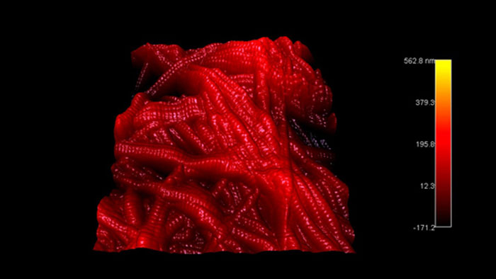
Single wall carbon nanotubes are transferred to an elastic PDMS substrate, then laterally compressed, causing the nanotubes to buckle into waves.
Scanned with a BudgetSensors Tap300Al-G AFM probe, 10 micron scan size
Image courtesy of Scott MacLaren, University of Illinois at Urbana-Champaign, USA
Anode oxidation of a Si substrate performed with a BudgetSensors ElectriTap300-G AFM probe on a JEOL JSPM-5200 AFM system
Scanned with a BudgetSensors Tap300E-G AFM probe, 4 micron scan size
Image courtesy of Takashi Sueyoshi JEOL Ltd, Japan
A thin strip of single layer graphene atop a ridged PDMS polymer substrate
Scanned with a BudgetSensors AIOAl AFM probe, soft tapping mode cantilever (C), 10 micron scan size
Image courtesy of Scott MacLaren, University of Illinois at Urbana-Champaign, USA
Phase image of a SEBS block copolymer, topography rendered in 3D, overlaid with the color data from the phase image
Scanned with a BudgetSensors Tap300Al-G AFM probe, 4 micron scan size
Image courtesy of Scott MacLaren, University of Illinois at Urbana-Champaign, USA
Thin film of Zein protein with cholesterol
Scanned with a BudgetSensors Tap300Al-G AFM probe, 15 micron scan size
Image courtesy of Scott MacLaren, University of Illinois at Urbana-Champaign, USA
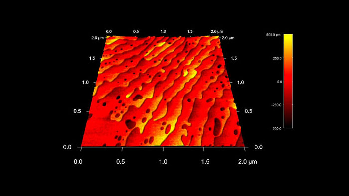
Atomic steps on a palladium surface
Scanned with a BudgetSensors Tap300Al-G AFM probe, 8 micron scan size
Image courtesy of Scott MacLaren, University of Illinois at Urbana-Champaign, USA
The curved surface of a human hair
Scanned with a BudgetSensors Tap300Al-G AFM probe, 35 micron scan tsize
Image courtesy of Scott MacLaren, University of Illinois at Urbana-Champaign, USA
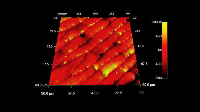
The surface of an ant's abdominal plating
Scanned with a BudgetSensors Tap300Al-G AFM probe, 90 micron scan size
Image courtesy of Scott MacLaren, University of Illinois at Urbana-Champaign, USA
Strontium titanium oxide (SrTiO3) surface with 4 Angstrom steps
Scanned with a BudgetSensors Tap300Al-G AFM probe, 2 micron scan size
Image courtesy of Scott MacLaren, University of Illinois at Urbana-Champaign, USA
Scanned with a OPUS by MikroMasch 240AC-NA AFM probe, 12 micron scan size
Image courtesy of Dr. Penka Terziyska, Innovative Solutions Bulgaria
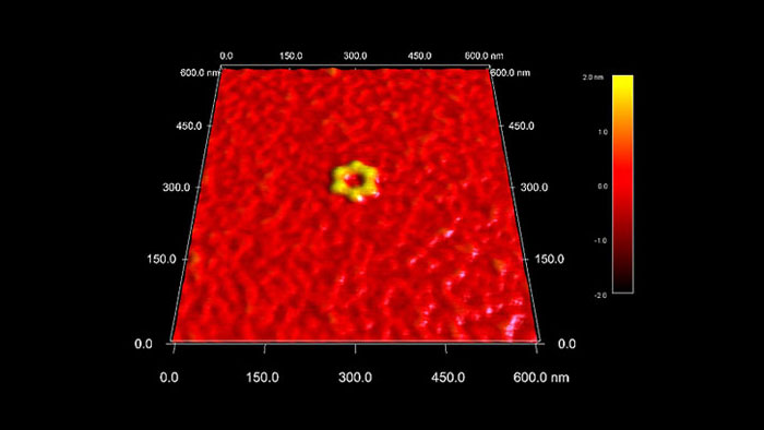
Hexagonal DNA nanostructure
Scanned with a BudgetSensors Tap300Al-G AFM probe, 600 nanometer scan size
Image courtesy of Scott MacLaren, University of Illinois at Urbana-Champaign, USA
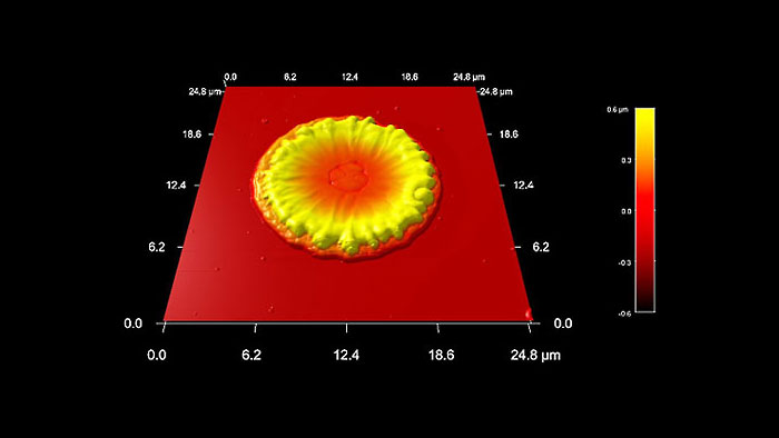
Silicon surface impacted with molten copper droplet from the exhaust of a spacecraft ion thruster
Scanned with a BudgetSensors Tap300Al-G AFM probe, 25 micron scan
Image courtesy of Scott MacLaren, University of Illinois at Urbana-Champaign, USA
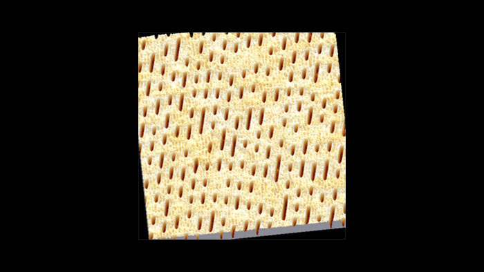
Information on compact discs (CDs) is stored by a binary pattern of real physical holes in the plastic surface just below the reflective aluminum foil. During recording (or 'burning') a CD these holes are literally burned in the plastic by the laser in the CD/DVD players in our PCs and laptops.
Scanned with a BudgetSensors Tap300-G AFM probe, 25 micron scan size
Image courtesy of Dr. Yordan Stefanov ISB, Bulgaria
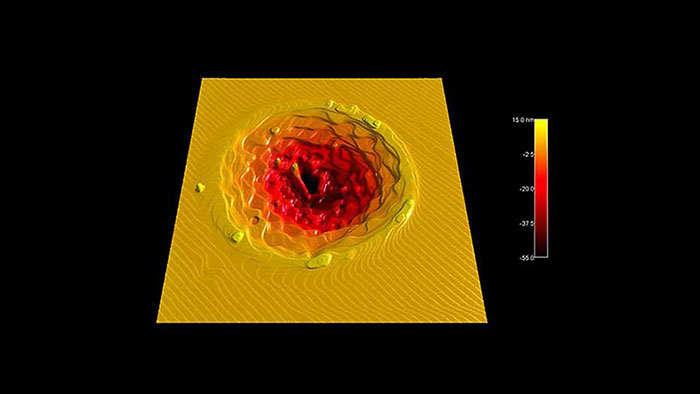
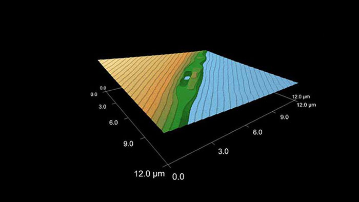
Crater in a sapphire substrate hit with a femtosecond laser pulse, followed by annealing to develop the step structure. The top surface is covered with single atomic steps (3Å).
Scanned with a BudgetSensors Tap300Al-G AFM probe, 20 micron scan size
Image courtesy of Scott MacLaren, University of Illinois at Urbana-Champaign, USA
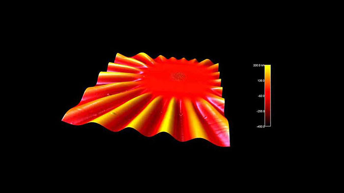
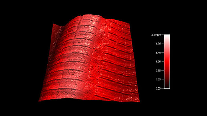
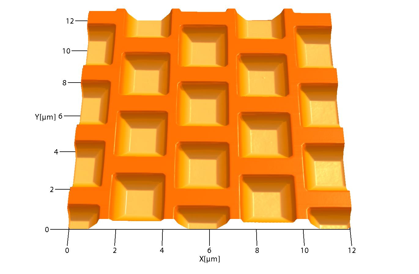
An extremely thin (30 nm) free standing silicon nitride membrane with nickel nanoparticles, following heating with a short laser pulse. The nanoparticles react with the substrate, and the induced stress in the film creates large ripples in the membrane surface
Scanned with a BudgetSensors Tap300Al-G AFM probe, 90 micron scan
Image courtesy of Scott MacLaren, University of Illinois at Urbana-Champaign, USA
Magnesium oxide (MgO) crystal, carved in a Focused Ion Beam (FIB) system. The top, unaltered surface shows single and double atomic steps.
Scanned with a BudgetSensors Tap300Al-G AFM probe, 20 micron scan size
Image courtesy of Scott MacLaren, University of Illinois at Urbana-Champaign, USA
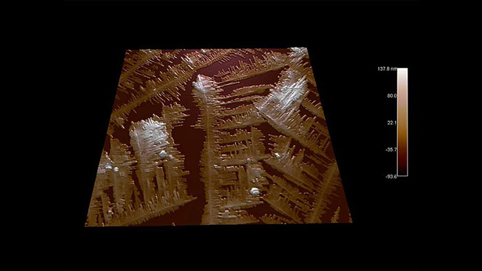
Crystallization of poly(benzyl-beta-L-glutamate) on glass
Scanned with a BudgetSensors Tap300Al-G AFM probe, 30 micron scan
Image courtesy of Scott MacLaren, University of Illinois at Urbana-Champaign, USA
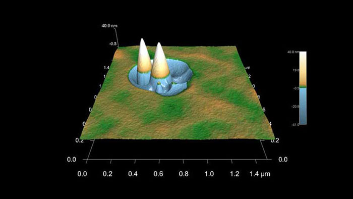
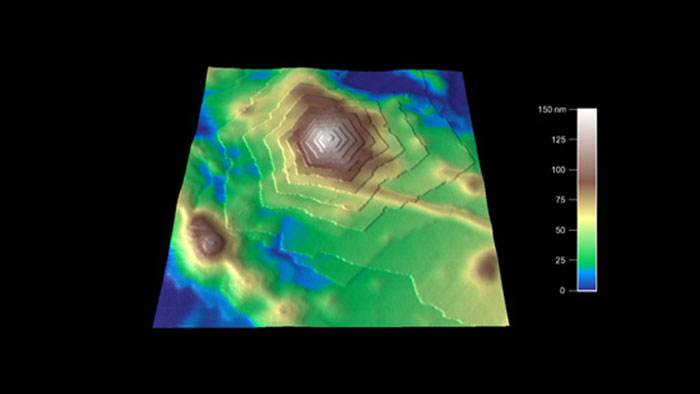
Contaminants on the surface prior to sputtering give rise to classic sputter cone formation.
Scanned with a BudgetSensors Tap300Al-G AFM probe, 1.5 micron scan
Image courtesy of Scott MacLaren, University of Illinois at Urbana-Champaign, USA
Sapphire crystal following annealing at 1400°C, leaving a clean surface with atomic steps and occasional defects. The steps are approximately 3Å tall.
Scanned with a BudgetSensors Tap300Al-G AFM probe, 12 micron scan size
Image courtesy of Scott MacLaren, University of Illinois at Urbana-Champaign, USA
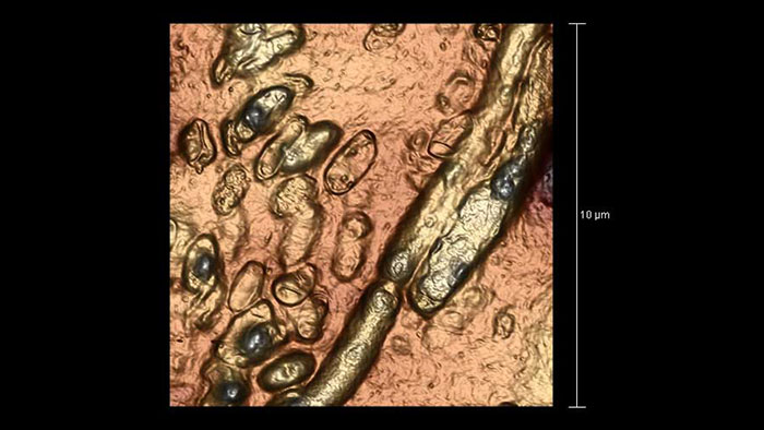
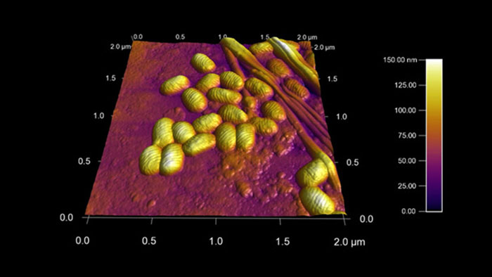
Xanthomonas campestris bacteria in potato agar
Scanned with a BudgetSensors Multi75-G AFM probe in light tapping mode, 10 micron scan size
Image courtesy of Dr. Yordan Stefanov, Innovative Solutions Bulgaria
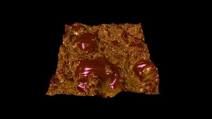
Chocolate is a complex material consisting primarily of a finely crystallized continuous fatty lipid matrix (cocoa butter) in which cocoa powder and sugar particles are dispersed. With time, the lipid crystals tend to merge to form larger crystals on a micron scale, significantly effecting the texture and taste of the chocolate. These images are of an aged commercial dark chocolate sample. The topography of the surface is rendered in 3D, while the coloring is an overlay of the phase image, which highlights the compositional differences (darker patches being the growing cocoa butter crystals).
Scanned with a BudgetSensors Tap300Al-G AFM probe, 15 micron scan size
Image courtesy of Scott MacLaren, University of Illinois at Urbana-Champaign, USA