Latest News

nanotools Variations of Collagen Properties Following Accumulation of Advanced Glycation End-products - news

Variations of Collagen Properties Following Accumulation of Advanced Glycation End-productsMon Mar 25 2024

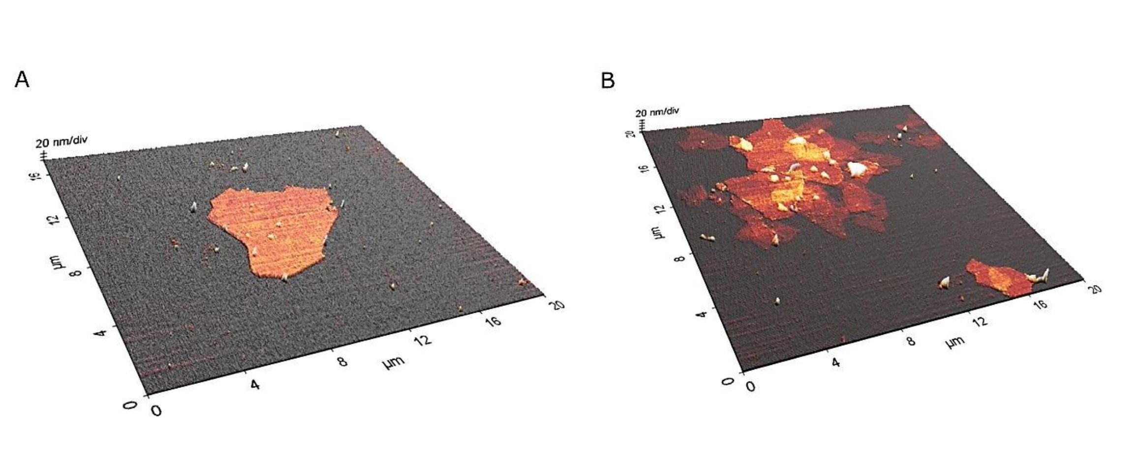
Discover how nanotools conical SSS-FMR with 2-3nm radius are applied for indentation measurements on collagen scaffolds.

  • Title: Modulation of the biophysical and biochemical properties of collagen by glycation for tissue engineering applications
  • DOI: 10.1016/j.actbio.2022.11.033
  • Authors: Mina Vaez, Meisam Asgari, Liisa Hirvonen, Gorkem Bakir, Emilie Khattignavong, Maya Ezzo, Sebastian Aguayo, Christina M. Schuh, Kathleen Gough, Laurent Bozec
  • Publication: Acta Biomaterialia
  • Publisher: Elsevier
  • Date: 1 January 2023

NanoAndMore NanoAndMore Japan at the Japan Applied Physics Society Spring Academic Lecture

NanoAndMore Japan is exhibiting at the 71st Spring Academic Conference of the Japan Society of Applied PhysicsFri Mar 22 2024

NanoAndMore Japan https://www.nanoandmore.jp/ is exhibiting at the 71st Spring Academic Conference of the Japan Society of Applied Physics
Please feel free to drop by our booth No. E145 to learn more about the many different #AFMprobe types we offer from many different manufacturers and feel free to discuss your #atomicforcemicroscopy applications with us.
22~25 March, 2024
Setagaya Campus, Tokyo City University https://meeting.jsap.or.jp/english
@JSAPmeeting @JSAP_official @JSAP_EXPO

NanoWorld Manipulating hyperbolic transient plasmons in a layered semiconductor - news

Manipulating hyperbolic transient plasmons in a layered semiconductorTue Mar 19 2024

Manipulating hyperbolic transient plasmons in a layered semiconductor
Anisotropic materials with oppositely signed dielectric tensors support hyperbolic polaritons, displaying enhanced electromagnetic localization and directional energy flow. * However, the most reported hyperbolic phonon polaritons are difficult to apply for active electro-optical modulations and optoelectronic devices. * In the nature communications letter “Manipulating hyperbolic transient plasmons in a layered semiconductor”, Rao Fu, Yusong Qu, Mengfei Xue, Xinghui Liu, Shengyao Chen, Yongqian Zhao, Runkun Chen, Boxuan Li, Hongming Weng, Qian Liu, Qing Dai and Jianing Chen report a dynamic topological plasmonic dispersion transition in black phosphorus (BP) via photo-induced carrier injection, i.e., transforming the iso-frequency contour from a pristine ellipsoid […]

NANOSENSORS Mitochondrial‐derived vesicles retain membrane potential and contain a functional ATP synthase - news

Mitochondrial‐derived vesicles retain membrane potential and contain a functional ATP synthaseFri Mar 15 2024

Vesicular transport is a means of communication. *
While cells can communicate with each other via secretion of extracellular vesicles, less is known regarding organelle‐to organelle communication, particularly in the case of #mitochondria . *
Mitochondria are responsible for the production of energy and for essential metabolic pathways in the cell, as well as fundamental processes such as apoptosis and aging. *
In the article “Mitochondrial‐derived vesicles retain membrane potential and contain a functional ATP synthase” Reut Hazan (Ben‐Menachem), Dvora Lintzer, Tamar Ziv, Koyeli Das, Irit Rosenhek‐Goldian, Ziv Porat, Hila Ben Ami Pilo, Sharon Karniely, Ann Saada, Neta Regev‐Rudzki and Orphry Pines show that functional mitochondria isolated from Saccharomyces cerevisiae release vesicles, independent of the fission machinery. *
They isolate these #mitochondrialderivedvesicles (MDVs) and find that they are relatively uniform in size, of about 100 nm, and carry selective protein cargo enriched for ATP synthase subunits. *
Imaging analyses of mitochondrial‐derived #vesicles by #atomicforcemicroscopy ( #AFM ) and transmission electron microscopy (TEM), verified that these vesicles are within a range of 50 to 200 nm diameter. *
Images were captured with atomic force microscopy using NANOSENSORS uniqprobe qp-BioAC-CI (CB2 or CB1 ) #AFMprobes. The qp-BioAC-CI AFM probes with their rounded AFM tips (typical AFM tip radius 30nm) on three soft #AFMcantilevers ( typical spring constant CB1: 0.3 N/m , typical spring constant CB2: 0.1 N/m, typical spring constant CB3: 0.06 N/m ) are especially designed for #cellimaging. *
Please find the full citation and a direct link to the full article in our NANOSENSORS blog

NanoWorld Studying the cation dependence of CO2 reduction intermediates at Cu by in situ VSFG spectroscopy - news

Studying the cation dependence of CO2 reduction intermediates at Cu by in situ VSFG spectroscopyFri Mar 08 2024

Studying the cation dependence of CO2 reduction intermediates at Cu by in situ VSFG spectroscopy
The nature of the electrolyte cation is known to have a significant impact on electrochemical reduction of CO2 at catalyst|electrolyte interfaces. An understanding of the underlying mechanism responsible for catalytic enhancement as the alkali metal cation group is descended is key to guide catalyst development. * In the article “Studying the cation dependence of CO2 reduction intermediates at Cu by in situ VSFG spectroscopy” Liam C. Banerji, Hansaem Jang, Adrian M. Gardner and Alexander J. Cowan use in situ vibrational sum frequency generation (VSFG) spectroscopy to monitor changes in the binding modes of the CO intermediate at the electrochemical interface […]

NANOSENSORS Correlation between the Dimensions and Piezoelectric Properties of ZnO Nanowires Grown by PLI-MOCVD with Different Flow Rates - news

Correlation between the Dimensions and Piezoelectric Properties of ZnO Nanowires Grown by PLI-MOCVD with Different Flow RatesMon Mar 04 2024

#Zincoxidenanowires (ZnO NWs) have gained considerable attention in the field of #piezoelectricity in the past two decades. However, the impact of growth-process conditions on their dimensions and polarity, as well as the piezoelectric properties, has not been fully explored, specifically when using pulsed-liquid injection metal–organic chemical vapor deposition (PLI-MOCVD). *
For the article “Correlation between the Dimensions and Piezoelectric Properties of ZnO Nanowires Grown by PLI-MOCVD with Different Flow Rates” Quang Chieu Bui, Vincent Consonni, Carmen Jiménez, Hervé Roussel, Xavier Mescot, Bassem Salem and Gustavo Ardila investigated the influence of the O2 gas and DEZn solution flow rates on the formation process of ZnO NWs and their related piezoelectric properties. *
While the length and diameter of ZnO NWs were varied by adjusting the flow-rate conditions through different growth regimes limited either by the O2 gas or DEZn reactants, their polarity was consistently Zn-polar, as revealed by #piezoresponseforcemicroscopy ( #PFM ) .*
Moreover, the piezoelectric coefficient of ZnO NWs exhibits a strong correlation with their length and diameter. The highest mean piezoelectric coefficient of 3.7 pm/V was measured on the ZnO NW array with the length above 800 nm and the diameter below 65 nm. These results demonstrate the ability of the PLI-MOCVD system to modify the dimensions of ZnO NWs, as well as their piezoelectric properties.*
NANOSENSORS™ conductive and wear-resistant Platinum-Silicide #AFMprobes of the PtSi-NCH type with a high spring constant (typical value 42 N/m) were used to mitigate the interference of the electrostatic effect during the measurements.*
In the DataCube PFM mode, the #AFMtip was systematically brought into contact with the sample at a determined position, subsequently held in 60 milliseconds for the piezoelectric measurement, and then retracted before proceeding to the next position. This sequential approach and retraction of the AFM tip was employed to avoid tip dragging during the scanning process, which could bend the NWs and cause a contact failure between the AFM tip and the sample. When the AFM tip was in contact with the sample, an AC voltage of 5 V amplitude and 15 kHz frequency of AC voltage was applied across the top and bottom of the sample through the tip and chuck of the AFM system. Due to the piezoelectric properties, the ZnO NWs were deformed in response to the AC voltage. This deformation was measured by the AFM tip to obtain the piezoelectric response amplitude and phase signals. The piezoelectric response amplitude is proportional to the piezoelectric coefficient, while the piezoelectric response phase identifies the polarity of ZnO NWs. Thanks to the small radius of the AFM tip, the piezoelectric response of each individual NW can be measured. By scanning the AFM tip across a 1 × 1 µm2 area, the piezoelectric response of the NWs in the array was mapped. For each sample, the piezoresponse amplitude values were extracted from the piezoresponse amplitude map, and the mean piezoresponse amplitude was evaluated to study the piezoelectric amplitude behavior of ZnO NWs grown at different flow rates.*

NanoWorld Structural and optical variation of pseudoisocyanine aggregates nucleated on DNA substrates - news

Structural and optical variation of pseudoisocyanine aggregates nucleated on DNA substratesTue Feb 27 2024

Structural and optical variation of pseudoisocyanine aggregates nucleated on DNA substrates
The ability to maximize the range of exciton transport while minimizing energy loss has significant implications for the design of future nanoscale light harvesting, optoelectronic, and sensing applications. * One method of achieving this would be to densely pack dyes into strongly coupled aggregates such that excitations can be coherently delocalized through the partial or full length of the aggregate. * Coherently coupled aggregates enable exciton migration over discreet spatial distances with near unitary quantum efficiency. As a result, controlled dye aggregation has long been studied by chemists as a method of tuning the photonic and physical properties of the […]

BudgetSensors Quantitative wear evaluation of tips based on sharp structures

Quantitative wear evaluation of tips based on sharp structuresMon Feb 26 2024

“This paper demonstrates the utility of sharp structures in assessing the topography of AFM tips and delves into the effects of scanning parameters on tip wear. A method employing BudgetSensors™ Tipcheck samples has been introduced to determine the shape and structure of AFM tips accurately. Based on its distinct features, the tip morphology can be non-destructively assessed using the AFM imaging mode. This offers a compelling alternative to the conventional SEM detection method. ”

NANOSENSORS Model of a graphite electrode - news

Model of a graphite electrodeFri Feb 23 2024

Interface analysis between a model for the graphite electrode and solvent for electrolytes of lithium-ion batteries. An example of the interface observation between highly oriented pyrolytic graphite (HOPG) as a model for graphite electrodes and tetraglyme, which has been studied as a solvent of electrolytes for lithium ion batteries. The AFM cantilever oscillation frequency and amplitude during the experiments were 92 kHz and 0.3 nm, respectively. The temperature was maintained at 298 K under an argon atmosphere throughout the experiment to prevent the dissolution of contaminants from the air, which could affect the interface structure. The topographic image revealed an ordered structure at Δf = 1000 Hz, obtained with tetraglyme adsorbed on an HOPG surface.
Scanned with a NANOSENSORS PointProbe® Plus PPP-NCHAuD AFM probe in FM mode.
Image courtesy of Dr. Taketoshi Minato, Institute for Molecular Science, National Institutes of Natural Sciences, Okazaki, Japan.

nanotools AFM Viscoelastic Quantification Over 5 Orders of Magnitude Frequency Range - news

AFM Viscoelastic Quantification Over 5 Orders of Magnitude Frequency RangeThu Feb 22 2024

Discover how nanotools biosphere™ with 2µm radius are applied to quantify the nanoscale loss tangent, storage modulus, and loss modulus of polymeric materials.
  • Title: Nanoscale rheology: Dynamic Mechanical Analysis over a broad and continuous frequency range using Photothermal Actuation Atomic Force Microscopy
    DOI: 10.1021/acs.macromol.3c02052
  • Authors: Alba R. Piacenti, Casey Adam, Nicholas Hawkins, Ryan Wagner, Jacob Seifert, Yukinori Taniguchi, Roger Proksch, and Sonia Contera
  • Publication: Macromolecules
  • Publisher: American Chemical Society
  • Date: January 16 2024

NanoWorld ACTIVE SELF-ASSEMBLY OF PIEZOELECTRIC BIOMOLECULAR FILMS VIA SYNERGISTIC NANOCONFINEMENT AND IN-SITU POLING - news

ACTIVE SELF-ASSEMBLY OF PIEZOELECTRIC BIOMOLECULAR FILMS VIA SYNERGISTIC NANOCONFINEMENT AND IN-SITU POLINGWed Feb 21 2024

Active self-assembly of piezoelectric biomolecular films via synergistic nanoconfinement and in-situ poling
Piezoelectric biomaterials have attracted great attention owing to the recent recognition of the impact of piezoelectricity on biological systems and their potential applications in implantable sensors, actuators, and energy harvesters. However, their practical use is hindered by the weak piezoelectric effect caused by the random polarization of biomaterials and the challenges of large-scale alignment of domains.* In the article “Active self-assembly of piezoelectric biomolecular films via synergistic nanoconfinement and in-situ poling” Zhuomin Zhang, Xuemu Li, Zehua Peng, Xiaodong Yan, Shiyuan Liu, Ying Hong, Yao Shan, Xiaote Xu, Lihan Jin, Bingren Liu, Xinyu Zhang, Yu Chai, Shujun Zhang, Alex K.-Y. Jen […]

MikroMasch Nanoendoscopy AFM is performed with modified OPUS 240AC-NG AFM probes

Nanoendoscopy AFM is performed with modified OPUS 240AC-NG AFM probes.Tue Feb 20 2024

Protocol for live imaging of intracellular nanoscale structures using atomic force microscopy with nanoneedle probes
“Atomic force microscopy (AFM) is capable of nanoscale imaging but has so far only been used on cell surfaces when applied to a living cell. Here, we describe a step-by-step protocol for nanoendoscopy-AFM, which enables the imaging of nanoscale structures inside living cells. The protocol consists of cell staining, fabrication of the nanoneedle probes, observation inside living cells using 2D and 3D nanoendoscopy-AFM, and visualization of the 3D data.”
Nanoendoscopy AFM is performed with modified OPUS 240AC-NG AFM probes.

NANOSENSORS Electron-beam lithography of nanostructures at the tips of scanning probe cantilevers - news

Electron-beam lithography of nanostructures at the tips of scanning probe cantileversFri Feb 16 2024

It is always exiting to see what our creative and innovative users are doing with our AFM probes.
In their article “Electron-beam lithography of nanostructures at the tips of scanning probe cantilevers” L. Forrer, A. Kamber, A. Knoll, M. Poggio and F. R. Braakman describe how they developed a process to fabricate nanoscale metallic gate electrodes on scanning probe cantilevers. *
They even patterned the very fragile tip of the NANOSENSORS AdvancedTEC ATEC-NC with a gate array defined through the etching process. *
Their method allows the patterning of nanoscale devices on fragile scanning probes, extending their functionality as sensors. *
Please have a look at the NANOSENSORS blog for the full citation and a direct link to the full article.

MikroMasch Lock-in Amplifier Based Peak Force Infrared Microscopy - NanoAndMore

Lock-in Amplifier Based Peak Force Infrared MicroscopyMon Jan 15 2024

Lock-in Amplifier Based Peak Force Infrared Microscopy
“[T]he current PFIR microscope requires customized hardware configuration and software programming for real-time signal acquisition and processing, which creates a high barrier to PFIR implementation. In this communication, we describe a type of lock-in amplifier-based PFIR microscopy that can be assembled with generic, commercially available equipment without special hardware or software programming.”
The measurements in PeakForce Infrared Microscopy mode are performed using our platinum coated HQ:NSC15/Pt AFM probes.

NANOSENSORS Happy Holidays from NANOSENSORS™ AFM probes - news

Happy Holidays from NANOSENSORS™ AFM probesSun Dec 24 2023

With this seasonal Special Development Christmas Tree AFM tip with a light snow coating, we would like to wish all users of our AFM probes Happy Holidays and a good start into the New Year!

We are looking forward to another year with you.


Loading
nanosensors-logo
nanoworld-logo
budgetsensors-logo
mikromasch-logo
opus-logo
sqube-logo
nanotools-logo