 Buy these AFM Probes together with other BudgetSensors AFM probes of your choice in a Budget Combo Box!


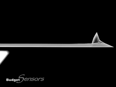
Micromachined monolithic silicon AFM probe for soft tapping mode operation.
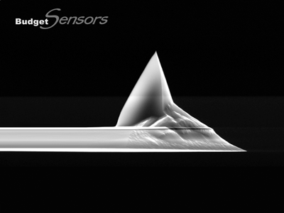
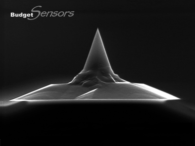
The consistent AFM tip radius of less than 10 nm ensures high resolution and good reproducibility. The rotated AFM tip provides more symmetric representation of high sample features.
The AFM probe features a reflective aluminum coating on the back side of the AFM cantilever. For measurements in liquids please use the back side gold coated Tap150GD-G or the overall gold coated Tap150GB-G!
With its industry standard dimensions of 3.4 x 1.6 x 0.3 mm the holder chip fits most commercial AFM systems.
Consistent high quality at a lower price!
This AFM probe features alignment grooves on the back side of the holder chip.

The first virus ever discovered and one of the most thoroughly researched, the tobacco mosaic virus (TMV) attacks various plant species and especially tobacco. The name of the rod-shaped RNA virus comes from the mosaic-like symptoms it causes.
Scanned with a BudgetSensors Tap150Al-G AFM probe, 5 micron scan size
Image courtesy of Dr. Yordan Stefanov, Innovative Solutions Bulgaria

A definite favorite of AFM researchers worldwide (or at least of the one who produced this image), Lindt’s 99% cocoa Excellence bar has very intense cocoa taste. The topography image of a bar’s back surface is rendered in 3D and overlaid with the phase image. The false-color yellowish spots are regions of growing cocoa butter crystals.
Scanned with a BudgetSensors Tap150Al-G AFM probe, 15 micron scan size
Image courtesy of Dr. Yordan Stefanov, Innovative Solutions Bulgaria; inspired by Scott MacLaren, UIUC, USA

Topography of CdSe thin film. Estimated mean nanocrystalline size is less than 10nm.
Scanned with a BudgetSensors Tap150Al-G AFM probe on a Bruker MultiMove V AFM system. 50 nanometer scan size
Image courtesy of Dr. Irina Bineva, Institute of Solid State Physics, BAS

Cd enriched areas in Zn0.4Cd0.6Se, topography and phase image. In order to obtain simultaneously good contrast in the phase image without distortion in the height image, due to surface damage, interleave mode with light tapping conditions for the height scan, and hard tapping for the phase image was used, repectively.
Scanned with a BudgetSensors Tap150Al-G AFM probe on a Bruker MultiMode V AFM system. 500 nanometer scan size
Image courtesy of Dr. Irina Bineva, Institute of Solid State Physics, BAS

Zn0.5Cd0.5Se thin film. Z axis max value is 16.6 nm.
Scanned with a BudgetSensors Tap150Al-G AFM probe on a Bruker MultiMode V AFM system, 1 micron scan size
Image courtesy of Dr. Irina Bineva, Institute of Solid State Physics, BAS
