 Buy these AFM Probes together with other BudgetSensors AFM probes of your choice in a Budget Combo Box!


Micromachined monolithic silicon AFM probe for force modulation (FM) and light tapping mode operation, and electric modes such as:
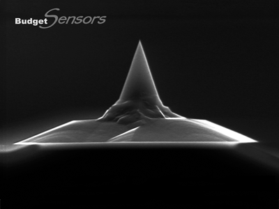
The consistent AFM tip radius of less than 25 nm ensures high resolution and good reproducibility. The rotated AFM tip provides more symmetric representation of high sample features.
The AFM probe features an overall chromium-platinum coating.
With its industry standard dimensions of 3.4 x 1.6 x 0.3 mm the holder chip fits most commercial AFM systems.
Consistent high quality at a lower price!
This AFM probe features alignment grooves on the back side of the holder chip.

Electrostatic Force Microscopy (EFM) test sample with differently biased metal lines. The topographic data (first image) shows two metal lines and the electrostatic force data helps distinguish between the biased line (left, 2 Volts) and the grounded one (right).
Scanned with a BudgetSensors Multi75E-G AFM probe in Electrostatic Force Microscopy mode, 7 micron scan size
Image courtesy of Dr. Yordan Stefanov, Innovative Solutions Bulgaria

Topography (left), PFM amplitude (center) and PFM phase (right) images of polycrystalline Pb(Zr0.3Ti0.7)O3 thin film
Scanned with a BudgetSensors Multi75E-G AFM probe in Piezoresponse Force Microscopy (PFM) mode, 1 micron scan size
Image courtesy of Prof. Yunseok Kim Sungkyunkwan University, South Korea

Tapping mode topography (left) and electrostatic force microscopy overlaid on topography (right) images of metal lines on an insulating substrate. EFM helps distinguish the two lines biased at 3V from the grounded one in the middle.
Scanned with a BudgetSensors Multi75E-G AFM probe, 10 micron scan size
Image courtesy of Dr. Yordan Stefanov, Innovative Solutions Bulgaria
