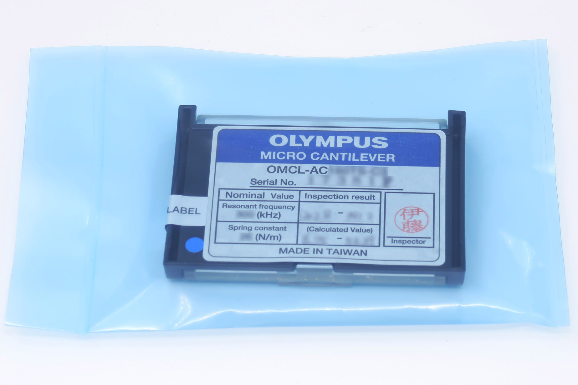


Exclusively from NanoAndMore, only as long as inventory lasts.
The OLYMPUS** OMCL-AC240TM series silicon AFM probes feature an AFM tip with ‘TipView structure’ that makes it easy to estimate the position of the AFM tip relative to the sample measurement site. The sharpened, tetrahedral, point-terminated AFM tip has very good symmetry when viewed from the front and is inclined when viewed from the side.
The OLYMPUS** OMCL-AC240TМ are most suitable for measurements of electrical properties such as Electrostatic Force Microscopy (EFM), Kelvin Probe Force Microscopy (KPFM) and Scanning Capacitance Microscopy (SCM).
The AFM tip and the tip side of the AFM cantilever are coated with platinum, which is a noble metal and exhibits good and stable conductivity. The back side of the AFM cantilever is coated with a thin aluminum reflective coating.
The parallel sidewalls of the holder chip make handling with tweezers easy and eliminate problems with chipping and debris. The holder chip does not feature alignment grooves.
Specifics Related to OLYMPUS** AFM Probes:
Last boxes. Exclusively from NanoAndMore and only as long as stock lasts.
Please contact us should you have any further questions.

PFM measurement of ultrathin (≈40 nm) poly(vinylidene fluoride-trifluoroethylene (PVDF-TrFE) film self-assembled on a monolayer (≈1 nm) graphene oxide (GO) film. a) Schematics showing the PFM experimental setup; b) PFM amplitude (scale bar is 1 μm) and c) PFM phase images representing stable bipolar remanent polarization states written in a box-like pattern on PVDF-NL (showing in plane and out of plane responses) using a conductive AFM cantilever (read voltage Vread = 2 V); d) Amplitude and phase SS-PFM hysteresis loops demonstrating ferroelectricity and large piezoresponse in PVDF-NL; e) PFM amplitude (amplitude sharply dropping at the 180° domain wall shown by arrows); f) phase profiles for the FE polarization states written in a box-like pattern with arrows indicating the polarization orientation.
Scanned with a OLYMPUS OMCL-AC240TM AFM probe on an Oxford Instruments MFP-3D Origin AFM system.
Image courtesy of Dr. Masamichi Yoshimura, Toyota Technological Institute

rGO samples were synthesized by Hydrothermal reduction of graphene oxide (GO), which is a promising approach for GO reduction since it is environmentally friendly, simple and cost effective. Before the hydrothermal treatment, a monolayer or a few-layer GO could be achieved after dispersing in water, in which the thickness of a single layer was measured to be 0.8–0.9 nm, as observed by AFM (Fig(a)). The GO layered structure was observed at the beginning of treatment. The number of layers reduces with the increase in reduction time, the layered nature becomes disordered, crumpled and smaller. rGO samples treated at (a) GO, rGO (b) 30 min, (c) 1 h, (d) 2 h, (e) 4 h, (f) 6 h, (g)8 h, (h) 10 h.
Scanned with a OLYMPUS OMCL-AC240TM AFM probe on a Bruker MutiMode 8 AFM system.
Image courtesy of Dr. Masamichi Yoshimura, Toyota Technological Institute

Height and current images of rGO films after 2 min and 6 min plasma irradiation and current profiles of green lines in the current images. Blue dotted line in AFM images shows the areas of 2nd layer of rGO flakes. A lower current was observed in the 2nd layer region than in the 1st layer at the irradiation time of 2 min. On the other hand, this tendency is reversed by irradiation for 6 min, and a higher current was observed in the 2nd layer region than in the 1st layer. As the irradiation time was extended, the second layer became more conductive than the 1st layer. Because the reduction by plasma treatment is taking place from the area exposed on the surface, at the short irradiation time, sufficient reduction has not occurred in the underlying GO layer. As the irradiation time was extended, the lower layer was reduced sufficiently by plasma.
Scanned with a OLYMPUS OMCL-AC240TM AFM probe on a Hitachi High-Tech Science NanoNaviⅡ AFM system.
Image courtesy of Dr. Masamichi Yoshimura, Toyota Technological Institute
