* The property ranges above, as well as the AFM Probe Guide, include NANOSENSORS™ Special Developments List AFM probes that might not be listed in the regular range of AFM probes on NanoAndMore. Please contact us if you can’t find the AFM probe you are looking for via the search field – we’ll assist you gladly!
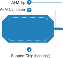
Comprehensive overview of NanoAndMore wide selection of available AFM probes classified by AFM tip, AFM cantilever and AFM support chip properties.
Overview of all different types of AFM tips classified by shape, material and coating. Discover the available AFM tips ranging from SuperSharpSilicon AFM tips for atomic resolution AFM imaging to the robust diamond coated AFM tips with extreme durability!
Overview of the different types of AFM cantilevers classified by shape, material and coating. NanoAndMore offer everything from thin triangular silicon nitride AFM cantilevers to short megahertz silicon AFM cantilevers for high speed scanning AFM.
Overview of the different types of AFM support chips classified by lateral dimensions, thickness, material and alignment grooves.
Some special AFM probes that do not fit into the standard classification pattern such as tipless AFM cantilevers, ultra AFM cantilevers, self sensing / self actuating AFM probes, etc.
Some special AFM probes that do not fit into the standard classification pattern such as tipless AFM cantilevers, ultra AFM cantilevers, self sensing / self actuating AFM probes, etc.
AFM videos and AFM scan images from our AFM probe suppliers.
Freeware apps courtesy of Dr. Joe Griffith, Bell Labs
Basic working principle of contact mode AFM. Change AFM scan parameters and see how the AFM system reacts.
See why AFM tip sharpness and aspect ratio are important for accurate visualization of small sharp features in AFM imaging.
Observe how the oscillation of the AFM probe piezo actuator is transferred to the AFM cantilever depending on frequency and damping!
General information about the technique Atomic Force Microscopy (AFM), as well as information on different AFM measurement modes, AFM system settings and other helpful tips.
Learn about the exciting technique for atomic resolution imaging and manipulation Atomic Force Microscopy! What is AFM? What is its operation principle? What AFM operation modes are there?
AFM is a powerful measurement technique. This note is a general overview of the basic steps needed for performing a successful topography AFM measurement in contact or tapping mode on an AFM system with optical cantilever deflection detection.
Images obtained by scanning a sample with an AFM tip are strongly dependent on the AFM tip geometry. AFM scans are a result of the convolution of the AFM tip and the surface. In order to understand how AFM images are formed and how they differ from the real surface topography, we need to know about AFM tip shape effects.
Before choosing the right probe, you first need to choose the right experiment. Check out this systematic guide, designed to help you make an informed decision!
Need to know how to setup your AFM system for a new AFM probe? Check out our step-by-step instruction on how to optimize AFM scan parameters on almost any AFM system, using almost any AFM probe.
Learn how to use Park Systems' own official Clip Type Chip Carrier in order to mount any standard AFM probe in Park AFM systems.
Тhe two most commonly used modes of AFM operation are contact mode and tapping mode. How do they differ? What are the advantages and disadvantages of each one?
If you ever wondered what rotated or standard AFM tips means and what difference the AFM tip shape has on your AFM measurements, here you can learn something about it.
A hot topic in AFM High Speed Scanning AFM (HSS AFM, HS AFM) measurements at up to video rates for in situ observation of dynamic processes. HSS AFM has been enabled by recent developments in instrumentation with high speed electronics and the development of advanced AFM cantilevers with megahertz resonance frequencies. Written by Dr.Ando of Kanazawa University.
Magnetic Force Microscopy (MFM) enables high-resolution imaging of the magnetic properties of different materials. When using an AFM probe with a magnetic coating on the tip side of the AFM cantilever, the AFM system can measure the magnetic field gradients above the sample surface.
Learn about applications of colloidal AFM probes, product types, sphere sizes and materials, and different AFM cantilevers to choose from.
Silicon AFM probes are ‘carved out’ from single-crystal silicon wafers. The wafers are patterned in a microfabrication process similar to the one used in silicon chip manufacturing. The fabrication process consists of more than 100 steps and it takes a couple of months to complete.
