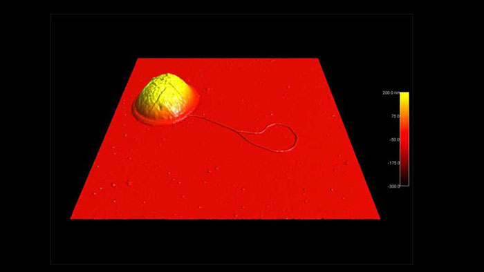
E-coli bacterium with flagellum
Scanned with a BudgetSensors Tap300Al-G AFM probe, 6 micron scan size
Image courtesy of Scott MacLaren, University of Illinois at Urbana-Champaign, USA
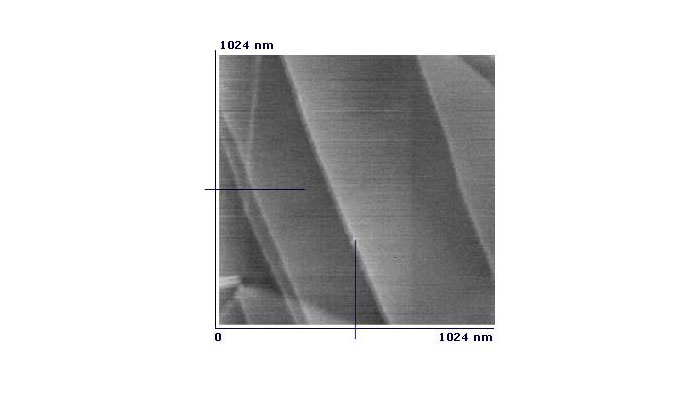
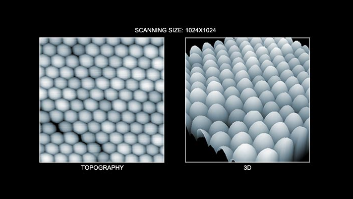
Highly Oriented Pyrolytic Graphite (HOPG) sample
Scanned with a BudgetSensors Tap300Al-G AFM probe, 1024 nanometer scan size
Image courtesy of Albert Lin, Angsnanotek Co., Ltd., Taiwan
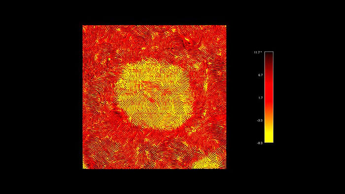
Phase image of a styrene-ethylene-butylene-styrene (SEBS) triblock copolymer
Scanned with a BudgetSensors Tap300Al-G AFM probe, 3 micron scan size
Image courtesy of Scott MacLaren, University of Illinois at Urbana-Champaign, USA
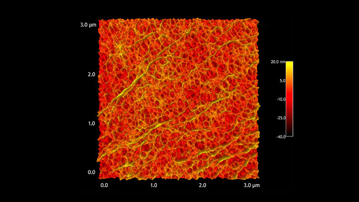
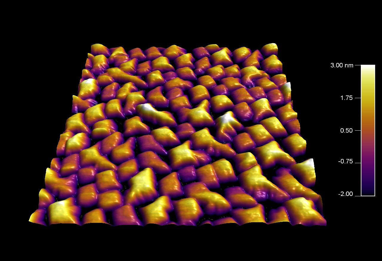
The porous surface of anodized aluminum
Scanned with a BudgetSensors Tap300Al-G AFM probe, 3 micron scan size
Image courtesy of Scott MacLaren, University of Illinois at Urbana-Champaign, USA
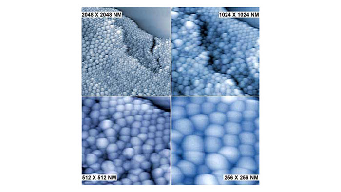
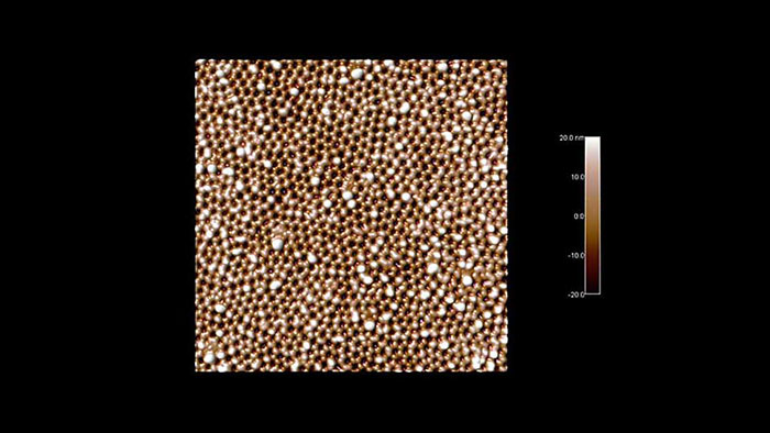
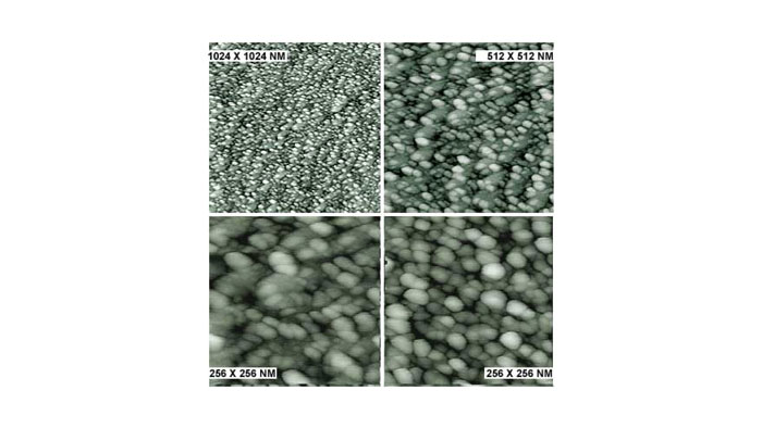
Zinc oxide nanoparticles (20~50nm)
Scanned with a BudgetSensors Tap300Al-G AFM probe, 2048, 1024, 512 and 256 nanometer scan size, respectively
Image courtesy of Albert Lin, Angsnanotek Co., Ltd., Taiwan
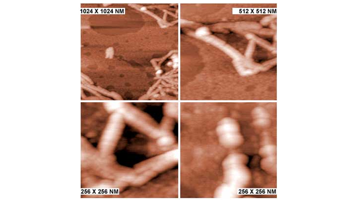
Amyloid fibrils (4~8nm)
Scanned with a BudgetSensors Tap300Al-G AFM probe, 1024 down to 256 nanometer scan size
Image courtesy of Albert Lin, Angsnanotek Co., Ltd., Taiwan
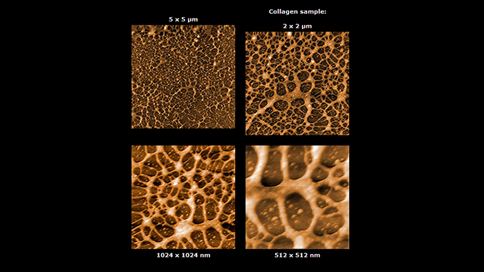
The blend of two biopolymers with compatibilizer
Scanned with a BudgetSensors Tap300Al-G AFM probe, 2 micron scan size
Image courtesy of Nagoya Municipal Industrial Research Institute Japan
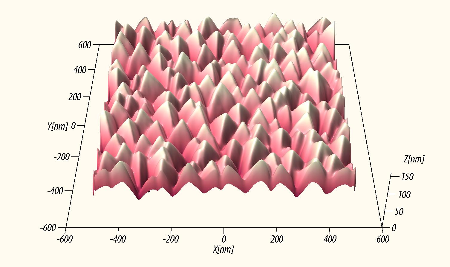
Screw dislocation in poly-oxy-methylene (POM)
Scanned with a BudgetSensors Tap300Al-G AFM probe, 3 micron scan size
Image courtesy of Jeff Kalish, University of Illinois at Urbana-Champaign, USA

Scanned with a BudgetSensors ElectriTap300-G AFM probe, 8 micron scan size
Image courtesy of Steve Liu, Dual Signal Tech Corp.

Surafece topography (left) and magnetic field (right) images of the surface of a magnetic ZIP disk
Scanned with a BudgetSensors MagneticMulti75-G AFM probe, 60 micron scan size
Image courtesy of Scott MacLaren, University of Illinois at Urbana-Champaign, USA

Topographic image (left) and Magnetic Force Microscopy (MFM) phase image (right) of a HDD platter surface. The high and low areas on the magnetic scan are regions with different orientation of the magnetic dipoles that store binary 1s and 0s.
Scanned with a BudgetSensors MagneticMulti75-G AFM probe in Magnetic Force Microscopy mode, 5 micron scan size
Image courtesy of Dr. Yordan Stefanov, Innovative Solutions Bulgaria

Electrostatic Force Microscopy (EFM) test sample with differently biased metal lines. The topographic data (first image) shows two metal lines and the electrostatic force data helps distinguish between the biased line (left, 2 Volts) and the grounded one (right).
Scanned with a BudgetSensors ElectriMulti75-G AFM probe in Electrostatic Force Microscopy mode, 7 micron scan size
Image courtesy of Dr. Yordan Stefanov, Innovative Solutions Bulgaria
Topography (left) and 3D topography (right) images of nanoparticles
Scanned with a BudgetSensors Tap300Al-G AFM probe, 1024 nanometer scan size.
Image courtesy of Albert Lin Angsnanotek Co., Ltd., Taiwan
Scanned with a BudgetSensors Tap300Al-G AFM probe. 5000, 2000, 1024 and 512 nanometer scan size, respectively
Image courtesy of Albert Lin, Angsnanotek Co., Ltd., Taiwan
Scanned with a BudgetSensors Tap300Al-G AFM probe. 2500, 1000 and 500 nanometer scan size, respectively
Image courtesy of Albert Lin, Angsnanotek Co., Ltd., Taiwan

Partially mixed and partially cured two component epoxy. The phase image data is overlaid on the 3D topography.
Scanned with a BudgetSensors Tap190Al-G AFM probe, 5 micron scan size
Image courtesy of Dr. Yordan Stefanov, Innovative Solutions Bulgaria
Imprints of different porphyrin aggregates in polystyrene
Scanned with a BudgetSensors Tap300Al-G AFM probe, 2.5 micron scan size
Image courtesy of Walter Smith, Haverford College, Haverford, USA
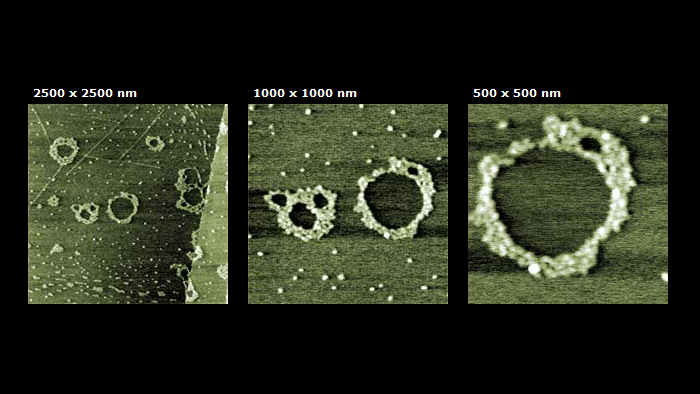
ZnO particles (<10nm)
Scanned with a BudgetSensors Tap300Al-G AFM probe, 1024, 512, 256 and 256 nanometer scan sizes, respectively
Image courtesy of Albert Lin, Angsnanotek Co., Ltd., Taiwan

Topography (left), PFM amplitude (center) and PFM phase (right) images of polycrystalline Pb(Zr0.3Ti0.7)O3 thin film
Scanned with a BudgetSensors ElectriMulti75-G AFM probe in Piezoresponse Force Microscopy (PFM) mode, 1 micron scan size
Image courtesy of Prof. Yunseok Kim Sungkyunkwan University, South Korea

Topography and 3D topography images of SrTiO3 single crystal substrate
Scanned with a BudgetSensors ContAl-G AFM probe in contact mode, 5 micron scan size
Image courtesy of Prof. Yunseok Kim Sungkyunkwan University, South Korea
Finely detailed surface of biaxially-oriented polypropylene (BOPP)
Scanned with a BudgetSensors Tap300Al-G AFM probe, 3 micron scan size
Image courtesy of Scott MacLaren, University of Illinois at Urbana-Champaign, USA
Scanned with a MikroMasch HQ:NSC19/Al BS AFM probe, 1200 nanometer scan size
Image courtesy of Dr. Penka Terziyska, Innovative Solutions Bulgaria

Scanned with a MikroMasch HQ:NSC14/Al BS AFM probe, 20 micron scan size
Image courtesy of Dr. Penka Terziyska, Innovative Solutions Bulgaria
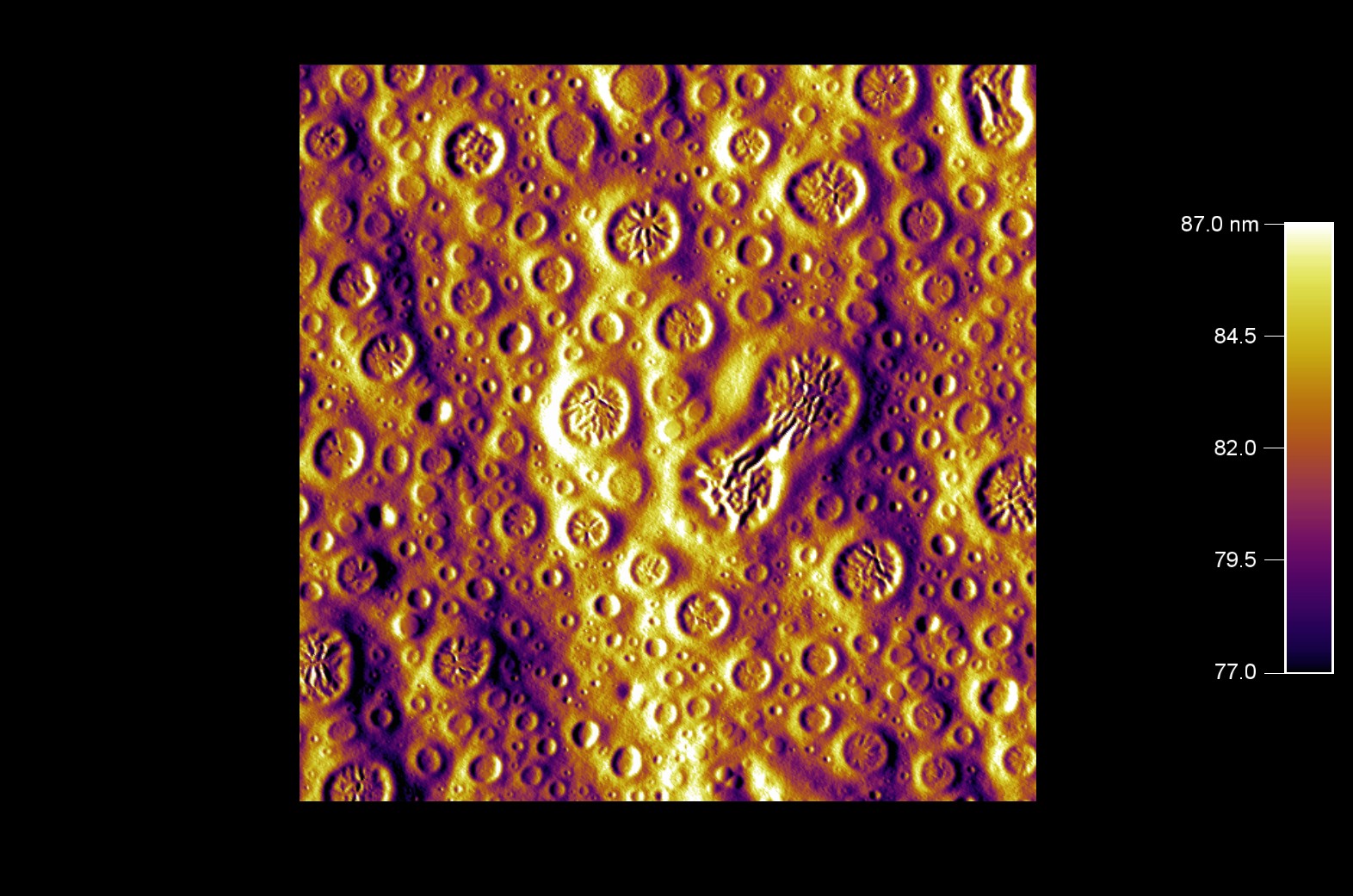
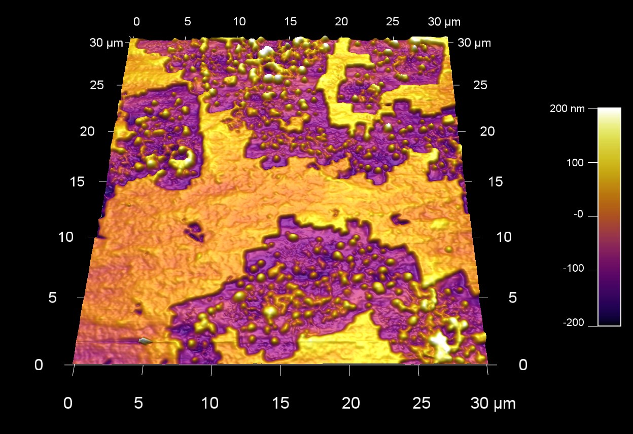
Dendritic growth of platinum nanoclusters
Scanned with a BudgetSensors Tap300Al-G AFM probe, 7 micron scan size
Image courtesy of Scott MacLaren, University of Illinois at Urbana-Champaign, USA
ZnO layer deposited on a silicon substrate by Atomic Layer Deposition. Sample provided by Dr. B. Blagoev, Institute of Solid State Physics – Bulgarian Academy of Sciences.
Scanned with a MikroMasch HQ:NSC15/Al BS AFM probe, 2 micron scan size
Image courtesy of Dr. Penka Terziyska, Innovative Solutions Bulgaria

Topography and 3D topography images of polycrystalline SrTiO3 single crystal substrate
Scanned with a BudgetSensors ContAl-G AFM probe in contact mode, 5 micron scan size
Image courtesy of Prof. Yunseok Kim, Sungkyunkwan University, South Korea

Kelvin Probe Measurement on graphene exfoliated on strontium titanate (SrTiO3) obtained in non-contact AFM mode using a frequency shift of -5 Hz. The graphene was irradiated with xenon 23+ ions under grazing incidence of 6°. On monolayer the impact of the ions lead to characteristic folding. In Bias-Image the exposed underlying substrate in this area can be clearly seen. Also, the monolayer shows lower surface potential difference to SrTiO3 than few monolayers.
Scanned with a BudgetSensors ElectriTap300-G AFM probe on a RHK Technology SPM 1000 Control System
Image courtesy of Benedict Kleine Bussmann, Oliver Ochedowski, Marika Schleberger AG Schleberger, University Duisburg-Essen
Scanned with a BudgetSensors Tap300Al-G AFM Probe, 2 micron scan
Image courtesy of Scott MacLaren, University of Illinois at Urbana-Champaign, USA
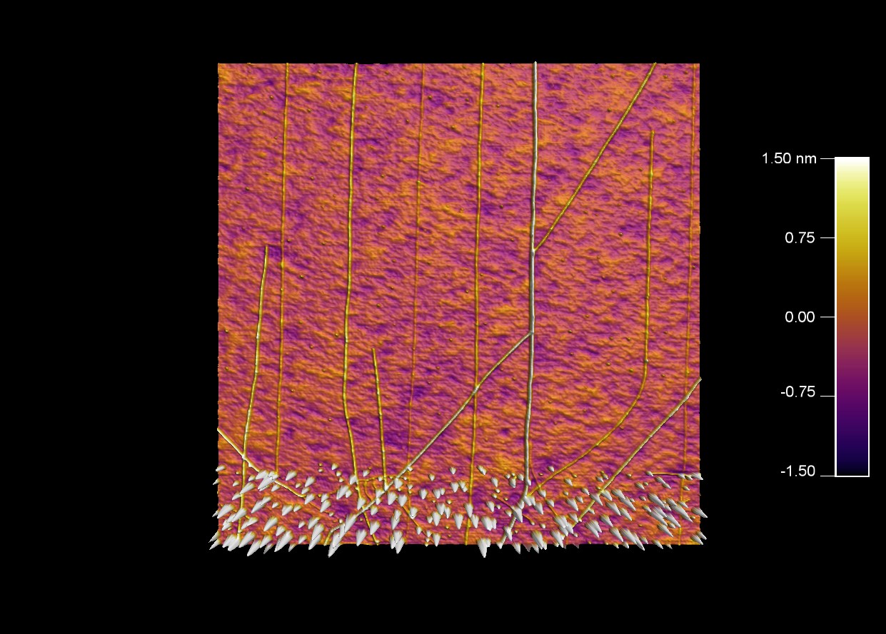
Carbon nanotubes and bundles emerging from line of catalyst particles
Scanned with a BudgetSensors Tap300Al-G AFM probe, 5 micron scan
Image courtesy of Scott MacLaren, University of Illinois at Urbana-Champaign, USA
Fast dried white glue.
Scanned with a BudgetSensors Tap300Al-G AFM probe, amplitude image, 10 micron scan
Image courtesy of Scott MacLaren, University of Illinois at Urbana-Champaign, USA
Scanned with a BudgetSensors Tap300Al-G AFM probe, 10 micron scan
Image courtesy of Scott MacLaren, University of Illinois at Urbana-Champaign, USA

Magnetic field image of high capacity (500 GB) hard disk
Scanned with a BudgetSensors MagneticMulti75-G AFM probe, 10 micron scan
Image courtesy of Scott MacLaren, University of Illinois at Urbana-Champaign, USA
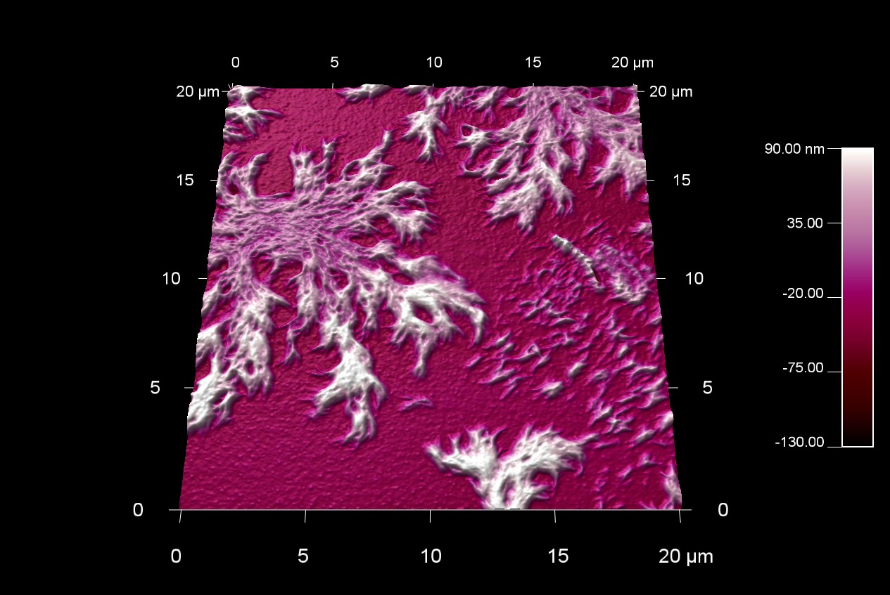
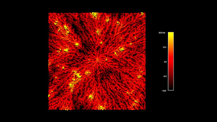
Dendritic growth of HDI polymer
Scanned with a BudgetSensors Tap300Al-G AFM probe, 20 micron scan
Image courtesy of Scott MacLaren, University of Illinois at Urbana-Champaign, USA
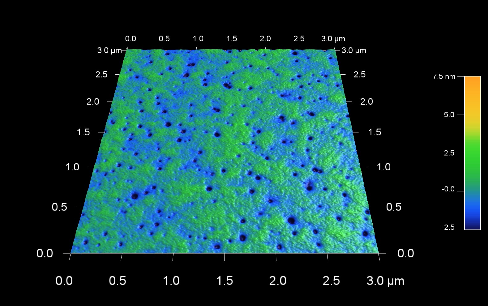
Scanned with a BudgetSensors Tap300Al-G AFM probe, 3 micron scan
Image courtesy of Scott MacLaren, University of Illinois at Urbana-Champaign, USA
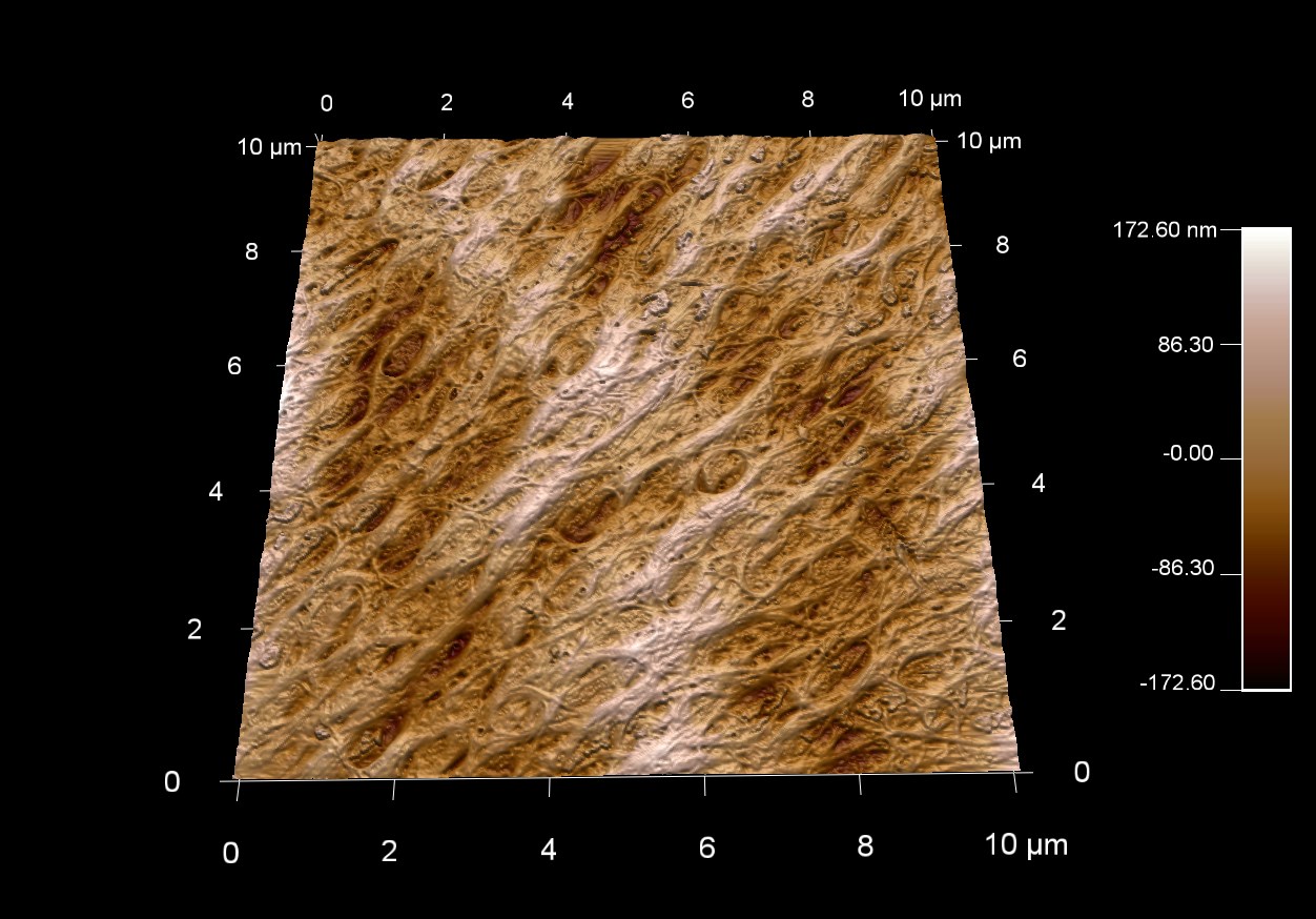
Polystyrene foam surface
Scanned with a BudgetSensors Tap300Al-G AFM probe, 30 micron scan
Image courtesy of Scott MacLaren, University of Illinois at Urbana-Champaign, USA
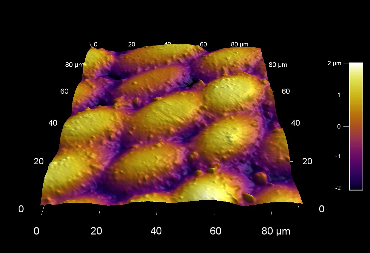
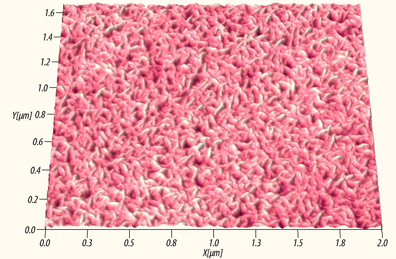
Sesame seed surface
Scanned with a BudgetSensors Tap300Al-G AFM probe, 90 micron scan
Image courtesy of Scott MacLaren, University of Illinois at Urbana-Champaign, USA