Latest News

NanoWorld Happy Birthday Switzerland - news

Happy Birthday SwitzerlandThu Aug 01 2019

Happy Birthday Switzerland (https://www.nanoworld.com/blog/happy-birthday-switzerland/?utm_source=Facebook&utm_medium=Blog&utm_content=Happy+Birthday+Switzerland&utm_campaign=NanoWorld+Blog) has been published on NanoWorld Blog. It's the Swiss National Holiday today. Have fun everyone!

NANOSENSORS Happy Swiss National Holiday with Smallest Swiss Cross - news

Happy Swiss National Holiday with Smallest Swiss CrossWed Jul 31 2019

Happy Swiss National Holiday with Smallest Swiss Cross on NANOSENSORS™ Blog Basel University: Smallest Swiss Cross - Made of 20 Single Atoms ( a NANOSENSORS™ PPP-NCL was used for this image) 20 bromine atoms positioned on a sodium chloride surface using the tip of an atomic force microscope at room temperature, creating a Swiss cross with the size of 5.6nm. The structure is stable at room temperature and was achieved by exchanging chlorine with bromine atoms. (Fig: University of Basel, Department of Physics)

NanoWorld Ultra-high resolution imaging of thin films and single strands of polythiophene using atomic force microscopy - news

Ultra-high resolution imaging of thin films and single strands of polythiophene using atomic force microscopyMon Jul 29 2019

Ultra-high resolution imaging of thin films and single strands of polythiophene using atomic force microscopy (https://www.nanoworld.com/blog/ultra-high-resolution-imaging-of-thin-films-and-single-strands-of-polythiophene-using-atomic-force-microscopy/?utm_source=Facebook&utm_medium=Blog&utm_content=Ultra-high+resolution+imaging+of+thin+films+and+single+strands+of+polythiophene+using+atomic+force+microscopy&utm_campaign=NanoWorld+Blog) has been published on NanoWorld Blog. Real-space images of polymers with sub-molecular resolution could provide valuable insights into the relationship between morphology and functionality of polymer optoelectronic devices, but their acquisition is problematic due to perceived limitations in atomic force microscopy (AFM).* In the article “Ultra-high resolution imaging of thin films and single strands of polythiophene using atomic force microscopy” Vladimir V. Korolkov, Alex Summerfield, Alanna Murphy, David B. Amabilino, Kenji Watanabe, Takashi Taniguchi and Peter H. Beton show that individual thiophene units and the lattice of semicrystalline spin-coated films of polythiophenes (PTs) may be resolved using AFM under ambient conditions through the low-amplitude (≤ 1 nm) excitation of higher eigenmodes of a cantilever.* They authors demonstrate that the use of higher eigenmodes in tapping-mode ambient AFM can be successfully employed to characterize both individual polymer strands down to a single-atom level and also the ordering of a semi-crystalline polymer with technological relevance. The combination of AFM and solution deposition provides a simple and high-resolution approach to characterizing the structure of polymers.* The use of NanoWorld Arrow-UHF high frequency AFM probes at their first eigenmode of ~1.4 MHz is mentioned.* https://www.nanoworld.com/ultra-high-frequency-tapping-mode-afm-tip-arrow-uhf Please have a look at the NanoWorld blogpost for the full citation and a direct link to the full article. #AtomicForceMicroscopy #ImagingTechniques #MolecularSelfAssembly

BudgetSensors SEM image of CS-20NG AFN calibration nanogrid standard

BudgetSensors® HS or CS calibration grating!Mon Jul 22 2019

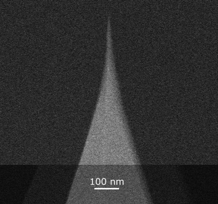
Get the most out of your BudgetSensors® HS or CS calibration grating! No surface is ideally smooth at the nanoscale, but that does not mean you cannot achieve highly accurate and precise calibration. Averaging the scan profile over several micrometers significantly improves your system's calibration. Check out our calibration gratings here: https://www.budgetsensors.com/calibration-standards 

NANOSENSORS Ferroelectricity-free lead halide perovskites – NANOSENSORS™ - news

Ferroelectricity-free lead halide perovskites – NANOSENSORS™Sun Jul 21 2019

Ferroelectricity-free lead halide perovskites on NANOSENSORS Blog. In the recent publication “Ferroelectricity-free lead halide perovskites” Andrés Gómez, Qiong Wang, Alejandro R. Goñi, Mariano Campoy-Quilesa and Antonio Abate describe how they employed direct piezoelectric force microscopy ( DPFM ) to examine whether or not lead halide perovskites exhibit ferroelectricity.* Their article aims to provide a deeper understanding of the fundamental physical properties of the organic–inorganic lead halide perovskites and solves a longstanding dispute about their non-ferroelectric character: an issue of high relevance for optoelectronic and photovoltaic applications.* In the course of their research in which besides using DPFM, they also employed piezoelectric force microscopy ( PFM ) and electrostatic force microscopy ( EFM ), they could demonstrate the non-ferroelectricity of lead halide perovskites. * The PFM images were acquired using a PtIr coated NANOSENSORS PPP-EFM AFM probe. https://www.nanosensors.com/PointProbe-Plus-Electrostatic-Force-Microscopy-PtIr5-Coating-afm-tip-PPP-EFM Please have a look at the NANOSENORS blog for the full citation and a direct link to the full article. #perovskite #photovoltaics #ElectrostaticForceMicroscopy #AFMprobes


Loading
nanosensors-logo
nanoworld-logo
budgetsensors-logo
mikromasch-logo
opus-logo
sqube-logo
nanotools-logo