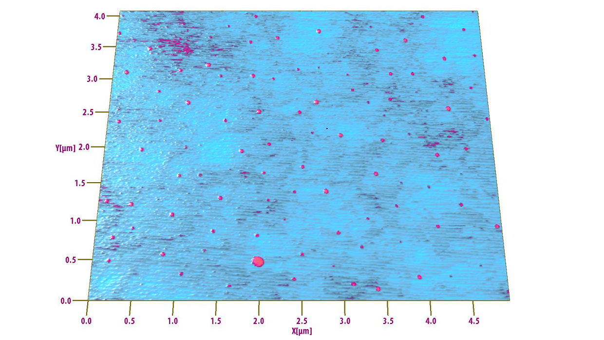
Topography image of erythrocytes (red blood cells)
Scanned with a MikroMasch XNC12/Cr-Au BS AFM probe, long cantilever in contact mode, 40 micron scan size
Image courtesy of Dr. Penka Terziyska, Innovative Solutions Bulgaria
Gallium antimonide (GaSb) quantum dots on gallium arsenide GaAs buffer layer obtained by liquid phase epitaxy. The height of the quantum dots is ~1nm.
Scanned with a MikroMasch HQ:NSC19/Al BS AFM probe in light tapping mode, 5 micron scan size
Image courtesy of Dr. Penka Terziyska, Innovative Solutions Bulgaria
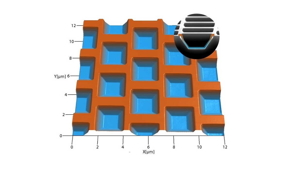
Topography image of the MikroMasch TGX calibration grating with undercut edges for lateral calibration and tip aspect ratio determination
Scanned with a OPUS by MikroMasch 240AC-NN AFM probe in light tapping mode, 12 micron scan size
Image courtesy of Dr. Penka Terziyska, Innovative Solutions Bulgaria
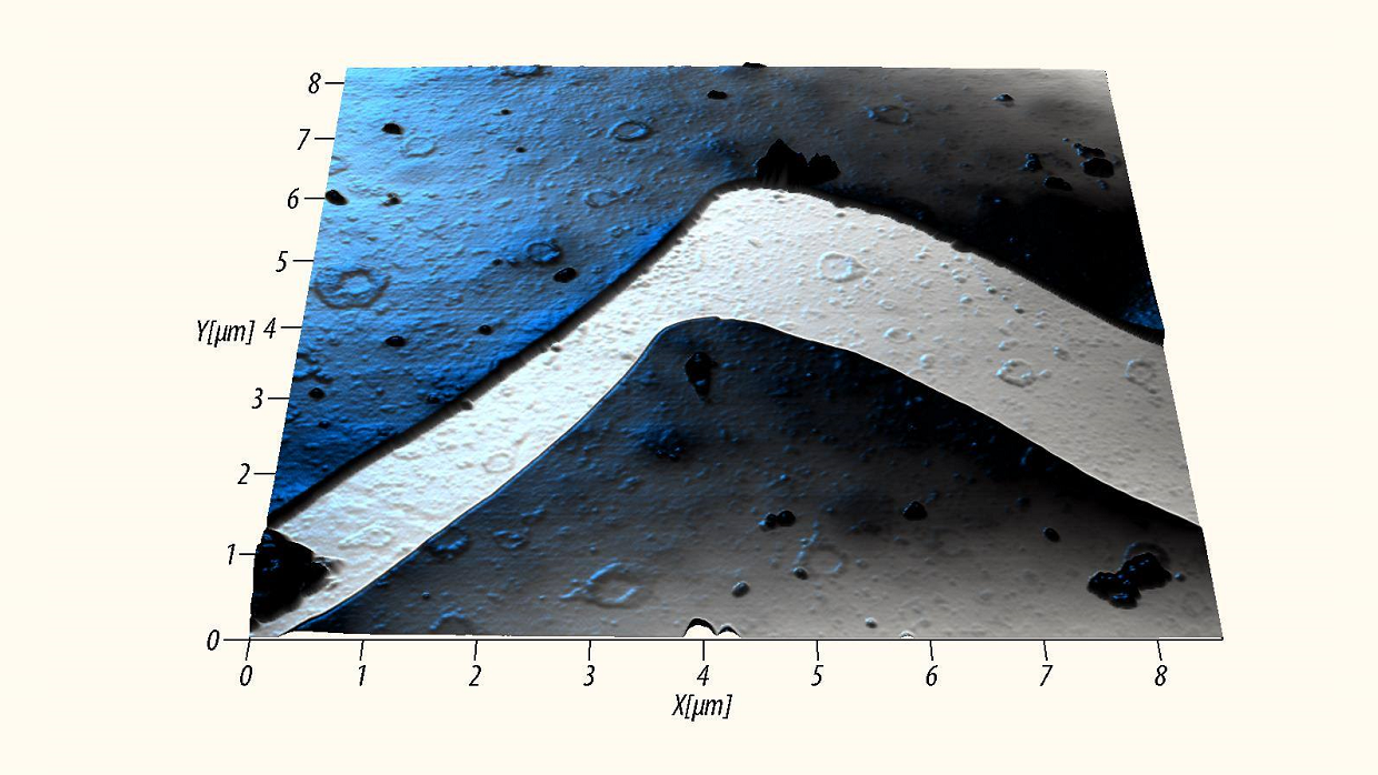
Crack in a carbon layer deposited on a glass substrate
Scanned with a MikroMasch HQ:NSC19/Al BS AFM probe, 8 micron scan size, 250 nanometer z-height
Image courtesy of Dr. Penka Terziyska, Innovative Solutions Bulgaria
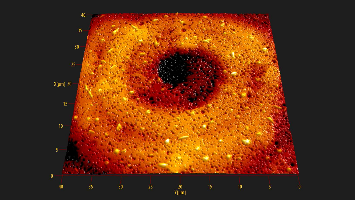
Central region of a self-organized Archimedean spiral pattern in a colloidal carbon film on glass. Sample provided by Dr. K. Shtarbova.
Scanned with a MikroMasch HQ:NSC19/Al BS AFM probe, 40 micron scan size
Image courtesy of Dr. Penka Terziyska, Innovative Solutions Bulgaria

Piezoelectric Force Microscopy (PFM) image of a single crystal, z-cut, Mg:LiNbO3. Ferroelectric domains written by applying -100V to the tip. Blue and yellow areas correspond to positive and negative polariszed domains.
Scanned with a MikroMasch HQ:NSC36/Pt AFM probe, short cantilever on an NT-MDT Solaris system; 30 micron scan size
Image courtesy of Dr. Martin Lilienblum, PhD Student at the Department of Materials, ETH Zurich, Switzerland

AFM non-contact mode topography image of LaAlO3 thin film on SrTiO3 single crystal. One step corresponds to 1 unit cell of SrTiO3 with a height of 0.3905nm.
Scanned with a MikroMasch HQ:NSC35/Al BS AFM probe, short cantilever on an NT-MDT Ntegra Prima system; 3x1.3 micron scan size
Image courtesy of Dr. Martin Lilienblum, PhD Student at the Department of Materials, ETH Zurich, Switzerland

Topography mage of the O-TiO2(110)-(1×1) surface. The bright and dark rows are O2c and Ti5c rows, respectively, and the bright spot is Oad. (f0=807 kHz, Q=23620, Δf=−70Hz, VDC=0.6V and A=500pm, image size: 3.5x2.0nm2). Experiments were performed with a home-built non-contact (NC) AFM system under ultra-high vacuum conditions (3x10^-11Torr) at 78K, which was operated in frequency modulation (FM). Scanned with a NANOSENSORS SD-T10L100 AFM probe, f0~800kHz.
Image courtesy of Prof. Yahiro Sugawara and Prof. Yan Jun Li, Department of Applied Physics, Graduate School of Engineering, Osaka University

Topography image (left) and Magnetic Force Microscopy (MFM) phase image (right) of an old 2.5” IBM-Hitachi DJSA-220 12GB hard disk platter. A NANOSENSORS Akiyama-probe with a custom magnetic coating is operated in frequency modulation, lift mode with lift height 70nm.
Scanned with a NANOSENSORS Akiyama-Probe in FM lift mode. Scan size 4 microns.
Image courtesy of Dr. Terunobu Akiyama, NANOSENSORS

Actin filament on Mica with APTES. Buffer: 100 mM KCl, 2 mM MgCl2, 1 mM EGTA, 20 mM Imidazole-HCl, pH7.6.
Scanned with a NanoWorld USC-F1.2-k0.15 AFM probe in High Speed Scanning mode. Scan size 250×250 nm2
Image courtesy of Prof. Kodera, nanoLSI, Kanazawa University, Japan

Actin filament on Mica with APTES. Buffer: 100 mM KCl, 2 mM MgCl2, 1 mM EGTA, 20 mM Imidazole-HCl, pH7.6.
Scanned with a NanoWorld USC-F1.2-k0.15 AFM probe in High Speed Scanning mode. Scan size 400×400 nm2
Image courtesy of Prof. Kodera, nanoLSI, Kanazawa University, Japan

Interface analysis between a model for the graphite electrode and solvent for electrolytes of lithium-ion batteries. An example of the interface observation between highly oriented pyrolytic graphite (HOPG) as a model for graphite electrodes and tetraglyme, which has been studied as a solvent of electrolytes for lithium ion batteries. The AFM cantilever oscillation frequency and amplitude during the experiments were 92 kHz and 0.3 nm, respectively. The temperature was maintained at 298 K under an argon atmosphere throughout the experiment to prevent the dissolution of contaminants from the air, which could affect the interface structure. The topographic image revealed an ordered structure at Δf = 1000 Hz, obtained with tetraglyme adsorbed on an HOPG surface.
Scanned with a NANOSENSORS PPP-NCHAuD AFM probe in a Shimadzu SPM-8000FM AFM system in FM mode.
Image courtesy of Dr. Taketoshi Minato, Institute for Molecular Science, National Institutes of Natural Sciences

Magneto-Conductive AFM (mC-AFM) measurements of Self-assembled monolayer (SAM) of overcrowded alkenes (OCAs) with ferromagnetic substrate. The Ni layer on the substrate worked as bottom electrode, and was magnetized by permanent magnet with maximum field ≈260mT under the substrate. A motor connected to the magnet rotated the magnet orientation externally, allowing to measure I-V profile of the SAM without moving the tip x-y location between up and down magnetization. After measuring ≥50 I–V curves with positive magnetic field, the AFM tip was lifted 40nm above the surface and the permanent magnet was rotated by 180°to apply negative magnetic field, immediately moving to the next measurement with negative field. Electric current was measured in contact mode by sweeping the bias voltage in the range ±1V. The applied force between the tip and the sample was kept at 180-190nN to avoid damage to the molecules. ≥50 I-V curves were averaged for each chirality-rotation step and two magnetic orientations.
Scanned with a NANOSENSORS CDT-FMR AFM probe on a Bruker Dimension Icon XR AFM system in PFT and contact mode.
Image courtesy of Dr. Taketoshi Minato, Institute for Molecular Science, National Institutes of Natural Sciences

Graphene oxide was synthesized from natural graphite by the modified Hummers’ method. AFM height images of mGO revealed the well-ordered flat tiling of mGO flakes (average size of 5 μm) with monolayer thickness of 1.2 nm. This process helped achieve a large area (≈1 cm2) mGO film, which was further utilized as 2D nucleation templates for fabricating large area ultrathin PVDF-NL (nano lamella).
Scanned with a BudgetSensors Tap300-G AFM probe on an Oxford Instruments MFP-3D Origin AFM system in AC mode.
Image courtesy of Dr. Masamichi Yoshimura, Toyota Technological Institute

PFM measurement of ultrathin (≈40 nm) poly(vinylidene fluoride-trifluoroethylene (PVDF-TrFE) film self-assembled on a monolayer (≈1 nm) graphene oxide (GO) film. a) Schematics showing the PFM experimental setup; b) PFM amplitude (scale bar is 1 μm) and c) PFM phase images representing stable bipolar remanent polarization states written in a box-like pattern on PVDF-NL (showing in plane and out of plane responses) using a conductive AFM cantilever (read voltage Vread = 2 V); d) Amplitude and phase SS-PFM hysteresis loops demonstrating ferroelectricity and large piezoresponse in PVDF-NL; e) PFM amplitude (amplitude sharply dropping at the 180° domain wall shown by arrows); f) phase profiles for the FE polarization states written in a box-like pattern with arrows indicating the polarization orientation.
Scanned with a OLYMPUS OMCL-AC240TM AFM probe on an Oxford Instruments MFP-3D Origin AFM system.
Image courtesy of Dr. Masamichi Yoshimura, Toyota Technological Institute

rGO samples were synthesized by Hydrothermal reduction of graphene oxide (GO), which is a promising approach for GO reduction since it is environmentally friendly, simple and cost effective. Before the hydrothermal treatment, a monolayer or a few-layer GO could be achieved after dispersing in water, in which the thickness of a single layer was measured to be 0.8–0.9 nm, as observed by AFM (Fig(a)). The GO layered structure was observed at the beginning of treatment. The number of layers reduces with the increase in reduction time, the layered nature becomes disordered, crumpled and smaller. rGO samples treated at (a) GO, rGO (b) 30 min, (c) 1 h, (d) 2 h, (e) 4 h, (f) 6 h, (g)8 h, (h) 10 h.
Scanned with a OLYMPUS OMCL-AC240TM AFM probe on a Bruker MutiMode 8 AFM system.
Image courtesy of Dr. Masamichi Yoshimura, Toyota Technological Institute

Height and current images of rGO films after 2 min and 6 min plasma irradiation and current profiles of green lines in the current images. Blue dotted line in AFM images shows the areas of 2nd layer of rGO flakes. A lower current was observed in the 2nd layer region than in the 1st layer at the irradiation time of 2 min. On the other hand, this tendency is reversed by irradiation for 6 min, and a higher current was observed in the 2nd layer region than in the 1st layer. As the irradiation time was extended, the second layer became more conductive than the 1st layer. Because the reduction by plasma treatment is taking place from the area exposed on the surface, at the short irradiation time, sufficient reduction has not occurred in the underlying GO layer. As the irradiation time was extended, the lower layer was reduced sufficiently by plasma.
Scanned with a OLYMPUS OMCL-AC240TM AFM probe on a Hitachi High-Tech Science NanoNaviⅡ AFM system.
Image courtesy of Dr. Masamichi Yoshimura, Toyota Technological Institute

We applied the formula of the elastic shell theory to successfully quantify the turgor pressure and cell wall elasticity of an onion epidermal cell using the cell curvature and apparent stiffness measured by AFM.
(A) Photographs of the cell measured before (left) and after (right) perforation. Yellow arrow indicates the perforation point. Cell lengths along long- and short- axes are denoted by La and Lb, respectively. Bars, 50 μm.
(B) Topographic images before (left) and after (right) perforation. Measurement area corresponds to the dashed box area in (A).
(C) Enlarged image of the perforation point.
(D) Cross-sectional graph of the cell wall surface before (red line) and after (blue line) perforation. Bulge height of the cell surface is denoted by w. Dashed lines are curves for curvature calculated from Lb and w.
(E) Quantities determined from AFM measurement. Mean curvature of the cell wall surface κM is calculated from La, Lb, and w.
Scanned with a NanoWorld NCHR AFM probe with 16 nm AFM tip radius for topography imaging on Bruker Nanowizard 4 AFM system (B,C).
Image courtesy of Dr.Yoichiro Hosokawa Nara Institute of Science and Technology

We applied the formula of the elastic shell theory to successfully quantify the turgor pressure and cell wall elasticity of an onion epidermal cell using the cell curvature and apparent stiffness measured by AFM.
(F) Force–indentation curves of the cell wall before (red dots) and after (blue dots) perforation. Dashed lines are fitting curves by the Hertz model and solid lines are fitting lines by the shell model.
(G) Apparent stiffness kas as a function of force F applied to the cell wall before (red dots) and after (blue dots) perforation. kas is estimated by linear least squares fitting of the force-indentation curve in the vicinity of F, as shown in (F). Bars on dots represent RMS error. Solid lines are exponential plateau curves: kas = 35 × {1 − exp(− F/7)} (red line); kas = 10 × {1 − exp(− F/1.28)} (blue line).
Scanned with NANOSENSORS™ SD-Sphere-NCH-S AFM probe with 400 nm AFM tip radius on Bruker Nanowizard 4 AFM system.
Image courtesy of Dr.Yoichiro Hosokawa Nara Institute of Science and Technology

We investigated the hydration structures of alkanethiol self-assembled monolayers terminated with a hydroxyl group using frequency-modulated atomic force microscopy. We observed two molecular structures, namely, the (√3 × √3) structure and the c(4 × 2) superlattice structure, and found that their hydration structures are different mainly because of the slight differences in their molecular arrangements. samples SAM(C11OH) on Au substrate (111) Buffer 0.1M Kcl
Scanned with a NANOSENSORS PPP-NCHAuD AFM probe on a Shimadzu SPM9600 AFM system modified for FM-AFM.
Image courtesy of Dr. Hirofumi Yamada Dr.Kei Kobayashi Kyoto University

α-Catenin molecule works as a tension sensor at cadherin-based adherens junctions, controlling intercellular tension. In this study, unfolding process of α-catenin under tension was explored by AFM-based molecular mechanical testing. "Mechano-adaptive sensory mechanism of α-catenin under tension" (https://www.nature.com/articles/srep24878) ©Koichiro Maki & Taiji Adachi, Kyoto University (Licensed under CC BY 4.0) Scanned with an OMCL-TR400PSA-1 AFM Probe on a Bruker AFM NanoWizard 3
Image courtesy of Dr. Koichiro Maki & Prof. Taiji Adachi, Kyoto University

Topography image of living cell (left), stiffness image(center) and zoom up of square area
Scanned with a OLYMPUS BL-AC40TS Bruker NanoWizard4 AFM, 100um scan Olympus
Image courtesy of Dr.Nagayama ,Ibaraki University of Japan