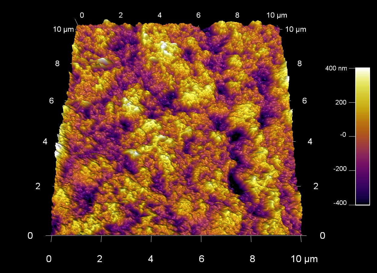
Scanned with a BudgetSensors Tap300Al-G AFM probe, 10 micron scan
Image courtesy of Scott MacLaren, University of Illinois at Urbana-Champaign, USA
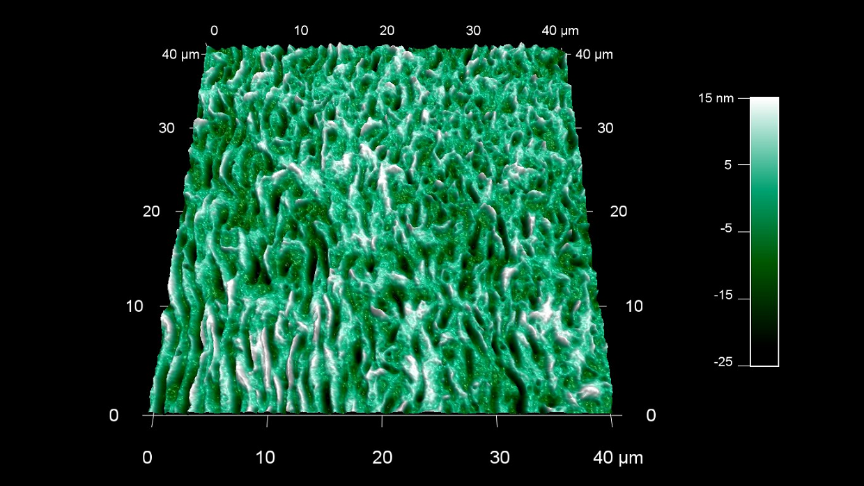
Ruptured gold palladium thin film
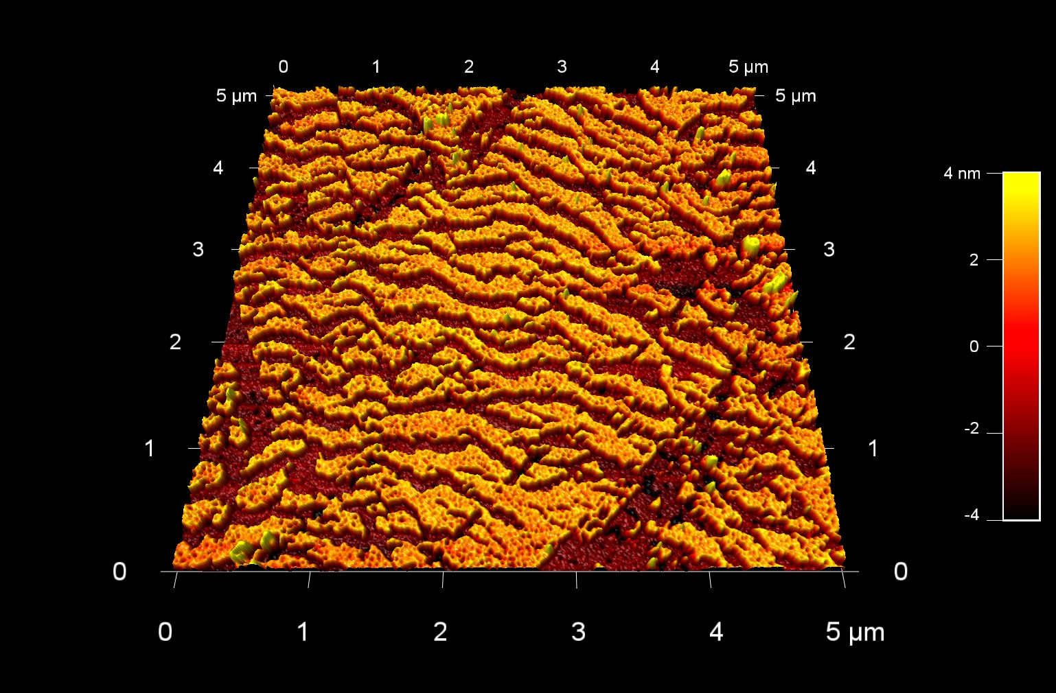
Scanned with a BudgetSensors Tap300Al-G AFM probe, 5 micron scan
Image courtesy of Scott MacLaren, University of Illinois at Urbana-Champaign, USA
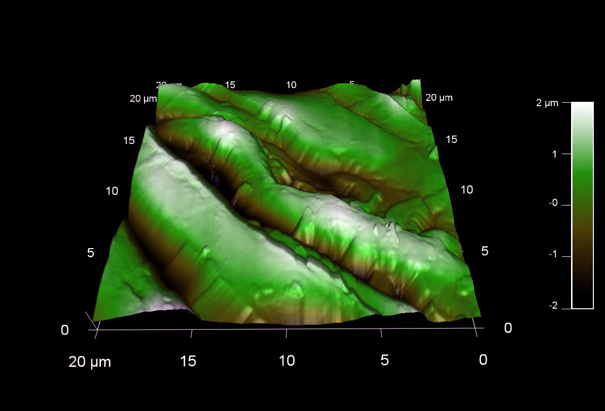
Two dimensional plastic optical grating
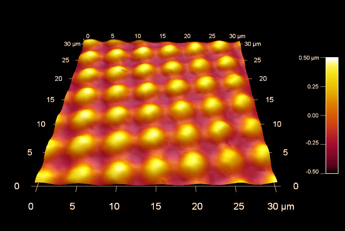
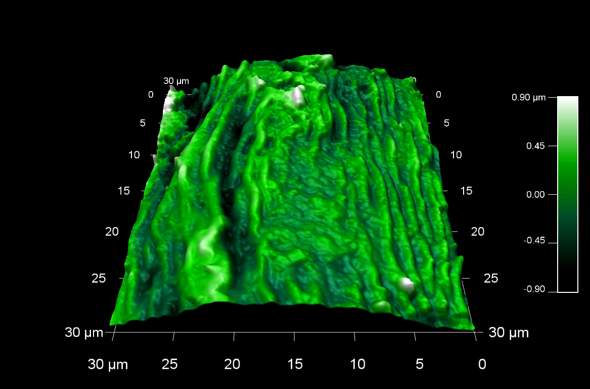
Scanned with a BudgetSensors Tap300Al-G AFM probe, 30 micron scan
Image courtesy of Scott MacLaren, University of Illinois at Urbana-Champaign, USA
Water etched gypsum crystal
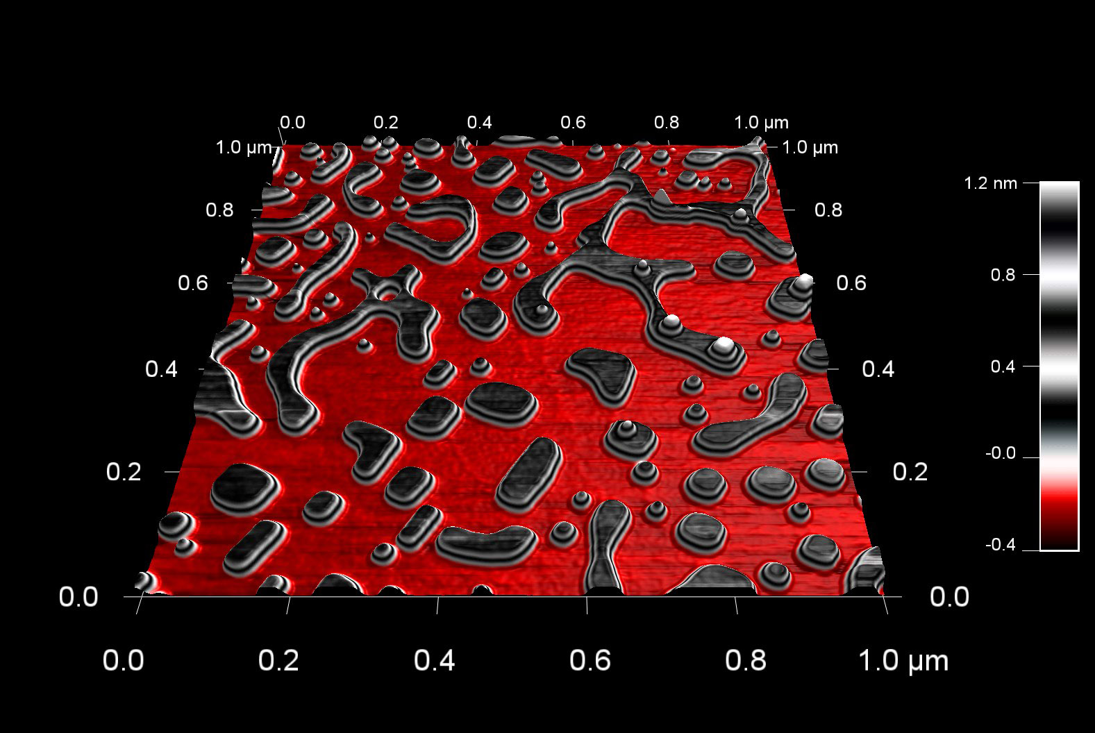
Scanned with a BudgetSensors Tap300Al-G AFM probe, 1 micron scan
Image courtesy of Scott MacLaren, University of Illinois at Urbana-Champaign, USA
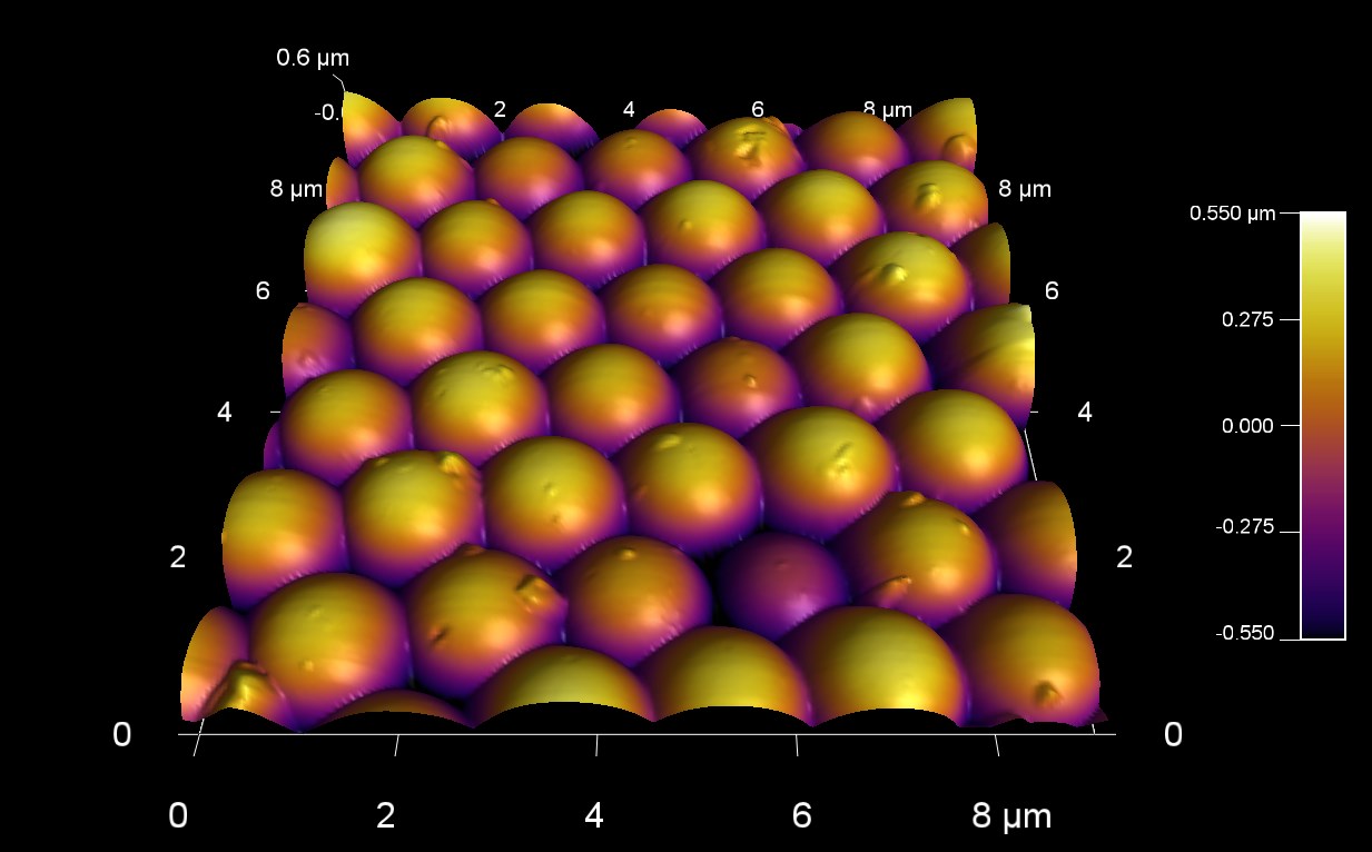
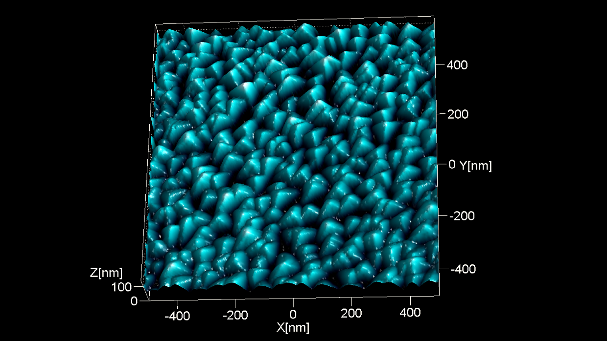
A scan of synthetic opal
Scanned with a BudgetSensors Tap300Al-G AFM probe, 9 micron scan
Image courtesy of Scott MacLaren, University of Illinois at Urbana-Champaign, USA
Scanned with a BudgetSensors Tap300Al-G AFM probe, 30 micron scan
Image courtesy of Scott MacLaren, University of Illinois at Urbana-Champaign, USA
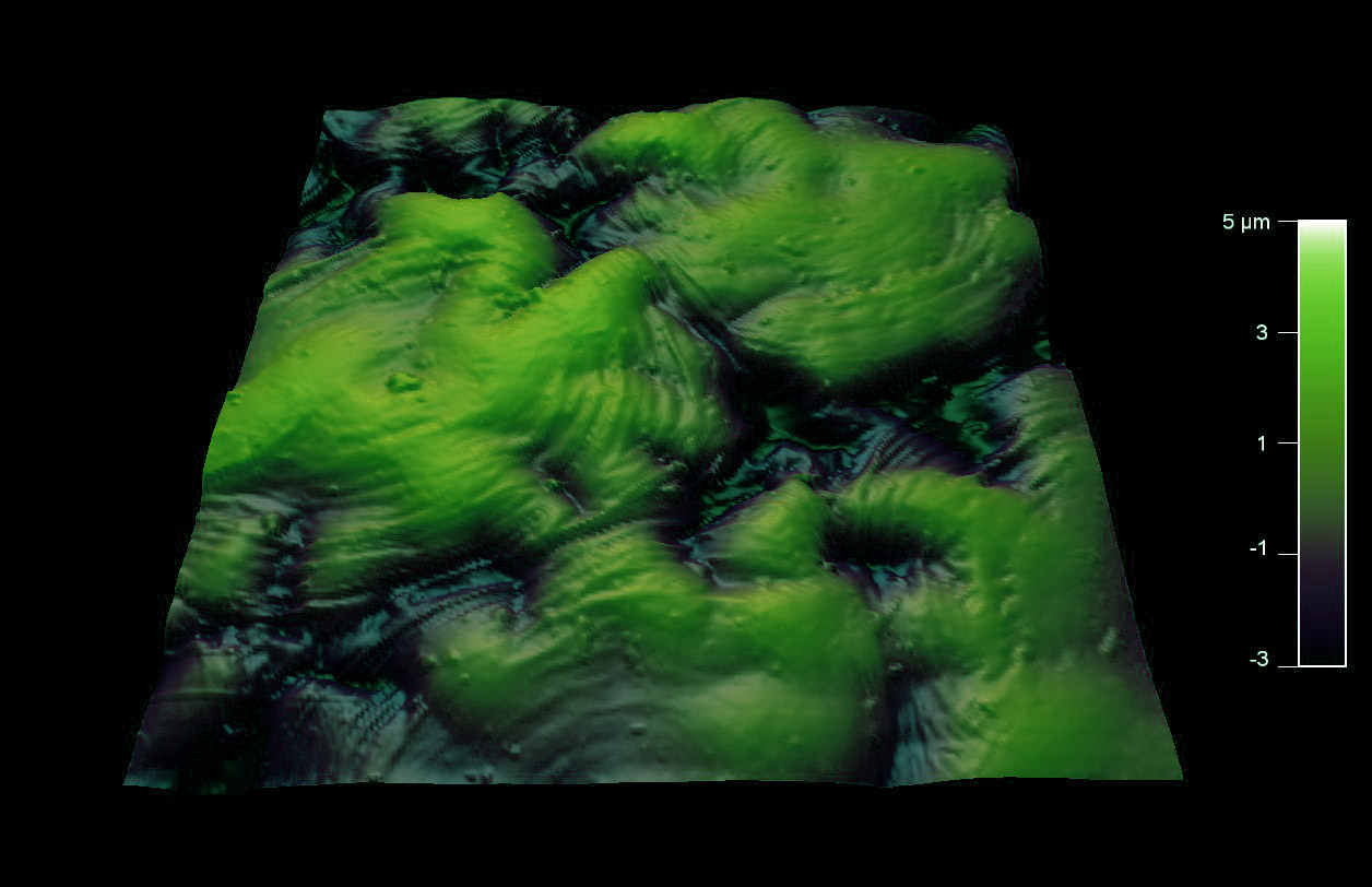
Polymer blend of polystyrene and polycaprolactone
Scanned with a BudgetSensors Tap300Al-G AFM probe, 10 micron scan
Image courtesy of Scott MacLaren, University of Illinois at Urbana-Champaign, USA
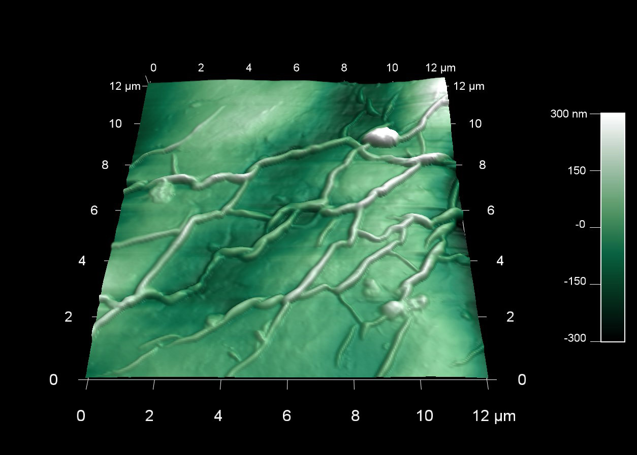
Scanned with a BudgetSensors Tap300Al-G AFM probe, 12 micron scan
Image courtesy of Scott MacLaren, University of Illinois at Urbana-Champaign, USA
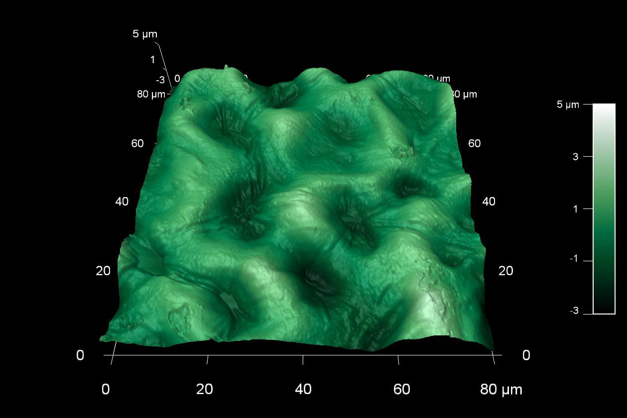
Scanned with a BudgetSensors Tap300Al-G AFM probe, 80 micron scan
Image courtesy of Scott MacLaren, University of Illinois at Urbana-Champaign, USA
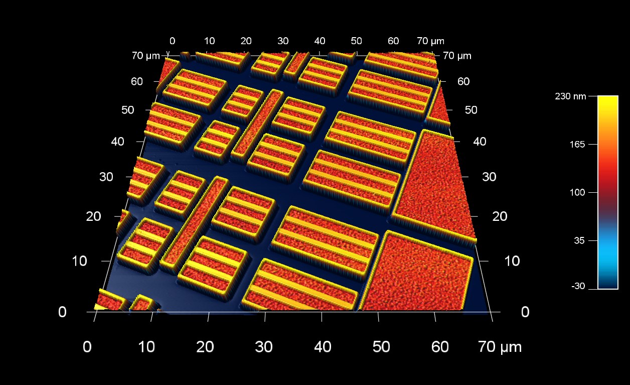
Scanned with a BudgetSensors Tap300Al-G AFM probe, 70 micron scan
Image courtesy of Scott MacLaren, University of Illinois at Urbana-Champaign, USA
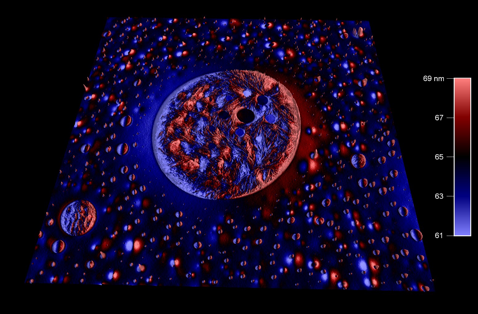
Scanned with a BudgetSensors Tap300Al-G AFM probe, 90 micron scan
Image courtesy of Scott MacLaren, University of Illinois at Urbana-Champaign, USA
Scanned with a BudgetSensors Tap300Al-G AFM probe, 90 micron scan
Image courtesy of Scott MacLaren, University of Illinois at Urbana-Champaign, USA
Scanned with a BudgetSensors Tap300Al-G AFM probe, 20 micron scan
Image courtesy of Scott MacLaren, University of Illinois at Urbana-Champaign, USA

An amplitude image of DNA plasmids
Scanned with a NANOSENSORS SSS-NCHR AFM probe, 1 micron scan
Image courtesy of Scott MacLaren, University of Illinois at Urbana-Champaign, USA

An amplitude image of DNA plasmids
Scanned with a NANOSENSORS SSS-NCHR AFM probe, 400 nm scan
Image courtesy of Scott MacLaren, University of Illinois at Urbana-Champaign, USA

The first virus ever discovered and one of the most thoroughly researched, the tobacco mosaic virus (TMV) attacks various plant species and especially tobacco. The name of the rod-shaped RNA virus comes from the mosaic-like symptoms it causes.
Scanned with a BudgetSensors Tap150Al-G AFM probe, 5 micron scan size
Image courtesy of Dr. Yordan Stefanov, Innovative Solutions Bulgaria

A definite favorite of AFM researchers worldwide (or at least of the one who produced this image), Lindt’s 99% cocoa Excellence bar has very intense cocoa taste. The topography image of a bar’s back surface is rendered in 3D and overlaid with the phase image. The false-color yellowish spots are regions of growing cocoa butter crystals.
Scanned with a BudgetSensors Tap150Al-G AFM probe, 15 micron scan size
Image courtesy of Dr. Yordan Stefanov, Innovative Solutions Bulgaria; inspired by Scott MacLaren, UIUC, USA

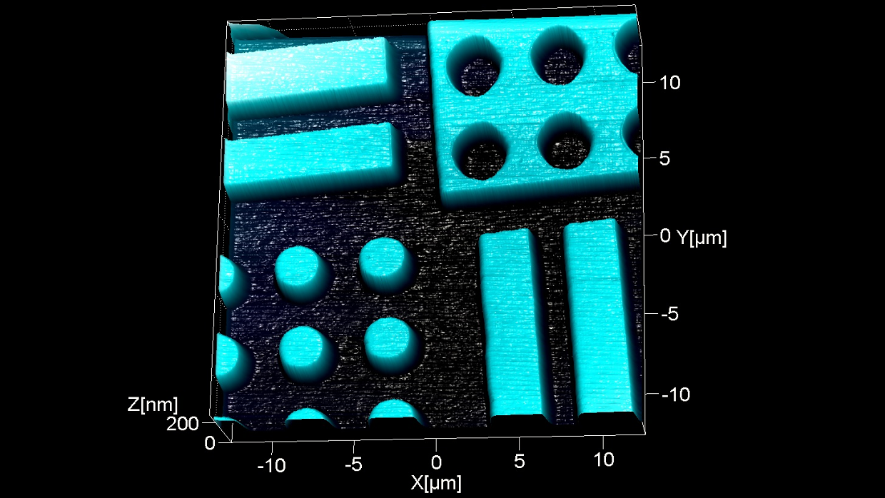
BudgetSensors CS-20NG calibration nanogrid. Structure-wise, the nanogrid differs from our microgrids by the additional array of circular holes with a 500 nanometer pitch. The images shows the transition between the microarrays and the nanoarray.
Scanned with a BudgetSensors AIOAl AFM probe, cantilever B (Multi75-like) in contact mode, 20 micron scan size
Image courtesy of Dr. Yordan Stefanov, Innovative Solutions Bulgaria

Tapping mode topography (left) and electrostatic force microscopy overlaid on topography (right) images of metal lines on an insulating substrate. EFM helps distinguish the two lines biased at 3V from the grounded one in the middle.
Scanned with a BudgetSensors Multi75E-G AFM probe, 10 micron scan size
Image courtesy of Dr. Yordan Stefanov, Innovative Solutions Bulgaria

This is a topography image of a holographic, UV optimized, blazed diffraction grating with 2400 lines/mm. It is a good graphic illustration of how much further at the nanoscale Atomic Force Microscopy allows us to ‘see’ beyond what any optical device could. The ridges diffract visible and near-UV light. To light these ridges are perfectly flat. The AFM using a sharp BudgetSensors tip shows us that their surface is actually quite rough.
Scanned with a BudgetSensors SiNi AFM probe, long cantilever in contact mode, 3 micron scan size
Image courtesy of Dr. Yordan Stefanov, Innovative Solutions Bulgaria
The TipCheck is BudgetSensors AFM probe tip evaluation sample. The sharp pyramidal structures allow reverse imaging of the tip apex.
Scanned with a BudgetSensors Tap300Al-G AFM probe, 1 micron scan size
Image courtesy of Dr. Yordan Stefanov, Innovative Solutions Bulgaria
Topography image of the central area of BudgetSensors height calibration standard HS-100MG with 100 nm nominal step height. The HS-100MG can also be used for X-Y calibration of large area scanners. The array design makes it possible to calibrate your AFM system without the need to rotate and realign the sample in-between X and Y axis calibration.
Scanned with a BudgetSensors Tap300Al-G AFM probe, 25 micron scan size
Image courtesy of Dr. Yordan Stefanov, Innovative Solutions Bulgaria

Tapping mode topography (left) and magnetic force microscopy overlaid on topography (right) images of the surface of a harddrive platter. MFM reveals the hidden bits of information stored by magnetizing small regions of a ferromagnetic film.
Scanned with a BudgetSensors Multi75M-G AFM probe, 10 micron scan size
Image courtesy of Dr. Yordan Stefanov, Innovative Solutions Bulgaria
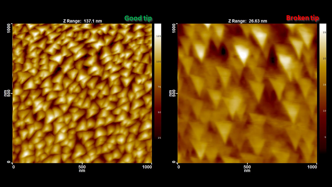
For accurate imaging of small features the AFM tip radius of curvature must be much smaller than the typical feature size. If, on the contrary, the AFM tip is much larger than the features, the result of the measurement is a reverse image of the AFM tip itself! On the left is a tapping mode scan with a brand new sharp AFM probe that reveals nicely the pyramidal structures on the TipCheck. On the right is a scan of the same TipCheck using a damaged AFM tip. The reverse-imaged triangular cross-section of the AFM tip pyramid, broken-off by improper probe handling, can be clearly recognized.
Scanned with a BudgetSensors Tap300Al-G AFM probe, 1 micron scan size
Image courtesy of Dr. Yordan Stefanov, Innovative Solutions Bulgaria
Did you know that collagen is the most abundant protein in our bodies making up around 30% of total protein content?
Scanned with a BudgetSensors Tap300Al-G AFM probe, 40 micron scan size
Image courtesy of Scott MacLaren, University of Illinois at Urbana-Champaign, USA
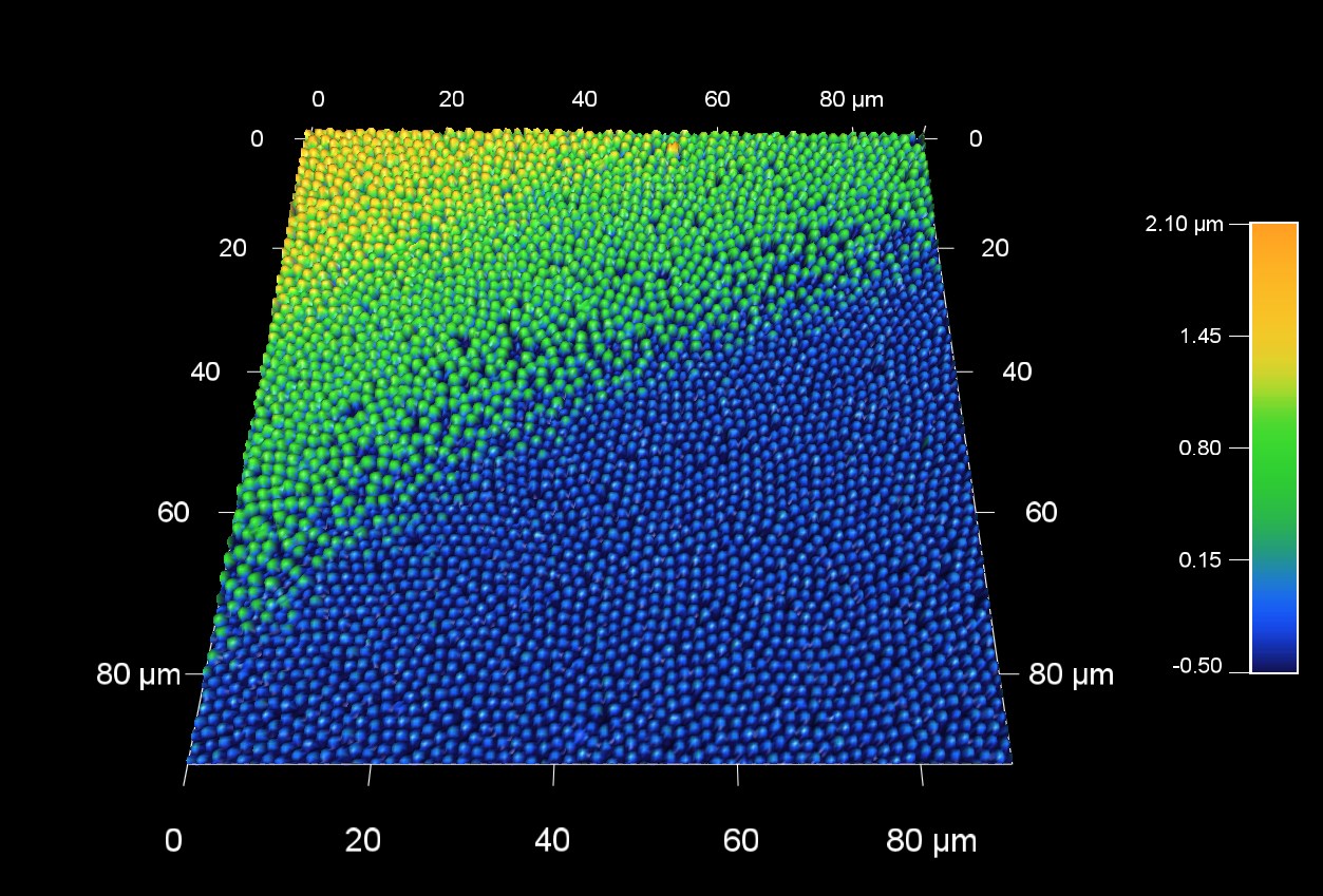
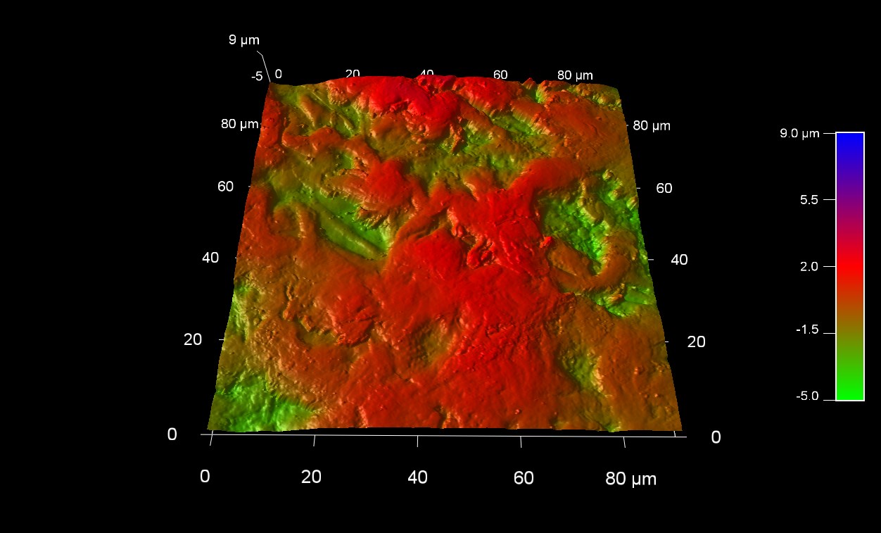
Precious opals are composed of closely packed silica spheres with sizes of several hundred nanometers. The beautiful colors of opals are caused by light diffraction and interference. This 90 micron AFM scan shows an opal surface with two transitions between neighboring planes of nanospheres.
Scanned with a BudgetSensors Tap300Al-G AFM probe, 90 micron scan size
Image courtesy of Scott MacLaren, University of Illinois at Urbana-Champaign, USA
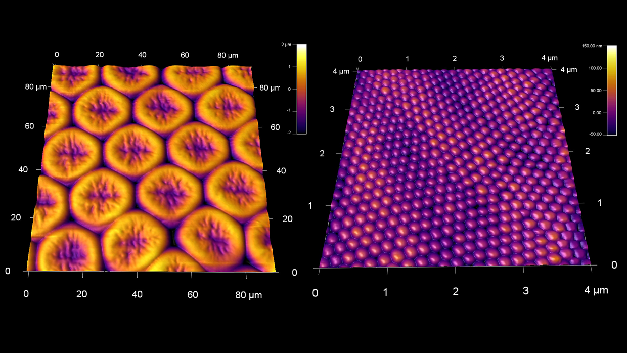
Large scale structure of a desiccated compound butterfly eye (left) and fine nanostructure completely covering the facets (right)
Scanned with a BudgetSensors Tap300Al-G AFM probe, 90 and 4 micron scan size, respectively
Image courtesy of Scott MacLaren, University of Illinois at Urbana-Champaign, USA

Contact mode topography image rendered in 3D and overlaid with the Lateral Force Microscopy image showing nicely the scales’ morphology as well as some hairspray droplets.
Scanned with a BudgetSensors ContAl-G AFM probe, 40 micron scan size
Image courtesy of Dr. Yordan Stefanov, Innovative Solutions Bulgaria

Information is stored on CDs by real physical holes in the plastic surface below the reflective aluminum foil. The laser holes on CD-Rs and DVD-Rs we 'burn' at home probably look a bit different from the molded ones on mastered CDs.
Scanned with a BudgetSensors Tap190Al-G AFM probe, 20, 10 and 2.5 micron scan size
Image courtesy of Dr. Yordan Stefanov, Innovative Solutions Bulgaria

Topography of the transition area between the shiny polished side of the blade and its sharpened cutting edge.
Scanned with a BudgetSensors AIOAl AFM probe, cantilever C (Tap150-like), 35 micron scan size
Image courtesy of Dr. Yordan Stefanov, Innovative Solutions Bulgaria

Topography scan of bacteria and negative imprints thereof in dried potato agar
Scanned with a BudgetSensors SiNi AFM probe, long cantilever, 10 micron scan size
Image courtesy of Dr. Yordan Stefanov, Innovative Solutions Bulgaria

The XC bacteria cause a number of diseases in plants. They are also used in the food industry to create the food additive xantham gum, a common thickening agent.
Scanned with a BudgetSensors Multi75Al-G AFM probe in light tapping mode, 10, 5 and 0.5 micron scan size
Image courtesy of Dr. Yordan Stefanov, Innovative Solutions Bulgaria

Topography image of human platelet acquired at room temperature
Scanned with a BudgetSensors ContAl-G AFM probe, 6 micron scan size
Image courtesy of Dr. Tonya Andreeva, Institute of Biophysics and Biomedical Engineering, BAS

Topography of CdSe thin film. Estimated mean nanocrystalline size is less than 10nm.
Scanned with a BudgetSensors Tap150Al-G AFM probe on a Bruker MultiMove V AFM system. 50 nanometer scan size
Image courtesy of Dr. Irina Bineva, Institute of Solid State Physics, BAS

Cd enriched areas in Zn0.4Cd0.6Se, topography and phase image. In order to obtain simultaneously good contrast in the phase image without distortion in the height image, due to surface damage, interleave mode with light tapping conditions for the height scan, and hard tapping for the phase image was used, repectively.
Scanned with a BudgetSensors Tap150Al-G AFM probe on a Bruker MultiMode V AFM system. 500 nanometer scan size
Image courtesy of Dr. Irina Bineva, Institute of Solid State Physics, BAS

Zn0.5Cd0.5Se thin film. Z axis max value is 16.6 nm.
Scanned with a BudgetSensors Tap150Al-G AFM probe on a Bruker MultiMode V AFM system, 1 micron scan size
Image courtesy of Dr. Irina Bineva, Institute of Solid State Physics, BAS