

Transparent electrodes based on molybdenum-titanium-oxide with increased water stability for use as hole-transport/hole-injection componentsSat May 04 2024
The application of #molybdenumoxide layers in electronic devices like #solarcells and #organiclightemittingdiodes (LEDs) has expanded considerably. *
Dielectric/metal/dielectric ( #DMD ) #transparentelectrodes based on #MoO3 have been applied in solar cells and organic light emitting diodes, by virtue of the favourable properties of MoO3 as hole-transport/hole-injection material.*
However, it was reported that poorly textured or amorphous MoO3 layers are extremely instable when exposed to ambient humidity and liquid water. *
In the article “Transparent electrodes based on molybdenum–titanium–oxide with increased water stability for use as hole-transport/hole-injection components” Selina Goetz, Rachmat Adhi Wibowo, Martin Bauch, Neha Bansal, Giovanni Ligorio, Emil List-Kratochvil, Christian Linke, Enrico Franzke , Jörg Winkler, Markus Valtiner and Theodoros Dimopoulos describe their study aimed to increase the water stability of sputtered, amorphous MoO3 layers without applying high temperatures, but by alloying with another refractory metal oxide to reduce hydrolysis and dissolution, while maintaining the essential electronic properties (i.e. wide band gap and high work function) of MoO3.*
In order to achieve this aim, the authors introduced titanium oxide to form a mixed molybdenum–titanium–oxide compound material. *
In contrast to the previous reports, the article by S. Goetz et al. introduces for the first time compact, amorphous #thinfilms, deposited by #sputtering from a mixed molybdenum–titanium–oxide (MTO) compound target. The sub-oxidic composition of the sputter target allows fast deposition in direct current (DC) magnetron mode, achieving high sputtering rates that are relevant for #industrialapplications. *
Selina Goetz et al. demonstrate that the addition of Ti strongly increases the stability in water, while the desirable electronic properties of MoO3, specifically the high work function and wide bandgap, are maintained. *
The DMD electrodes, with Ag as metal layer, were fabricated on both rigid and flexible substrates, namely glass and polyethylene terephthalate (PET). *
The obtained electrodes have low sheet resistance around 5 Ω/sq and high average visible transmittance well above 0.7 (including the substrate). As a result of the MTO stability, processing with water-based solutions takes place without electrode degradation. *
To demonstrate the process compatibility for large-scale, industrial production, the DMDs were sputter-deposited by a roll-to-roll process on a 300 mm-wide PET foil, achieving similar electrode properties with the laboratory-scale samples. *
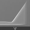
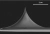
The #surfacecharacterization by #atomicforcemicroscopy was performed with a commercially available #atomicforcemicroscope using NANOSENSORS SuperSharpSilicon™ SSS-NCHR silicon high-resolution #AFMprobes for tapping mode with a typical #AFMtip radius of 2 nm.
Please have a look at the NANOSENSORS blog for the full citation and a direct link to the full article.


Bi2Se3 interlayer treatments affecting the Y3Fe5O12 (YIG) platinum spin Seebeck effectThu May 02 2024
Bi2Se3 interlayer treatments affecting the Y3Fe5O12 (YIG) platinum spin Seebeck effect
Spin Seebeck effects (SSE) arise from spin current (magnon) generation from within ferri-, ferro-, or anti-ferromagnetic materials driven by an applied temperature gradient. *
Longitudinal spin Seebeck effect (LSSE) investigations, where the spin current and temperature gradient evolve along a common z axis, while the magnetic field is applied in the y axis and the voltage contacts are spaced along the x axis, have become the most popular spin Seebeck device architecture. *
In article “Bi2Se3 interlayer treatments affecting the Y3Fe5O12 (YIG) platinum spin Seebeck effect”, Yaoyang Hu, Michael P. Weir, H. Jessica Pereira, Oliver J. Amin, Jem Pitcairn, Matthew J. Cliffe, Andrew W. Rushforth, Gunta Kunakova, Kiryl Niherysh, Vladimir Korolkov, James Kertfoot, Oleg Makarovsky and Simon Woodward present a method to enhance the longitudinal spin Seebeck effect at platinum/yttrium iron garnet (Pt/YIG) interfaces. *
The introduction of a partial interlayer of bismuth selenide (Bi2Se3, 2.5% surface coverage) interfaces significantly increases (by ∼380%–690%) the spin Seebeck coefficient over equivalent Pt/YIG control devices. *
Optimal devices are prepared by transferring Bi2Se3 nanoribbons, prepared under anaerobic conditions, onto the YIG (111) chips followed by rapid over-coating with Pt. The deposited Pt/Bi2Se3 nanoribbon/YIG assembly is characterized by scanning electron microscope. The expected elemental compositions of Bi2Se3 and YIG are confirmed by energy dispersive x-ray analysis. *
A spin Seebeck coefficient of 0.34–0.62 μV/K for Pt/Bi2Se3/YIG is attained for the authors’ devices, compared to just 0.09 μV/K for Pt/YIG controls at a 12 K thermal gradient and a magnetic field swept from −50 to +50 mT. *
Superconducting quantum interference device magnetometer studies indicate that the magnetic moment of Pt/Bi2Se3/YIG treated chips is increased by ∼4% vs control Pt/YIG chips (i.e., a significant increase vs the ±0.06% chip mass reproducibility). *
Increased surface magnetization is also detected in magnetic force microscope studies of Pt/Bi2Se3/YIG, suggesting that the enhancement of spin injection is associated with the presence of Bi2Se3 nanoribbons. *
To understand the surface magnetization effects in sample BSYIG1-a further, magnetic force microscope (MFM) measurements were undertaken using a commercial atomic force microscope and magnetic NanoWorld Pointprobe® MFMR AFM probes. *
MFM differs from traditional atomic force microscopy in that the AFM probe, in addition to providing a surface height profile, is also able to detect the magnetic field gradient above the sample. *
MFM surface profiling of BSYIG1-a revealed that a typical ribbon is comprised of multilayers of Bi2Se3, providing thicker sections ca. 250 nm thick [e.g., the profile along vector 1 in Figs. 3(a) and 3(b) cited below] and additional thinner sections ca. 100 nm thick [e.g., the profile along vector 2 in Figs. 3(a) and 3(b)]. Re-running ribbon profiles 1 and 2 with the magnetic probe at a height of 100 nm above the topological surface provided data on the magnetic field gradient variation along the same line profiles. The MFM amplitude [Figs. 3(c) and 3(d) cited below] increases over the Bi2Se3 flake, and furthermore, the magnetic enhancement correlates with the thickness of the Bi2Se3, being larger for the thicker part of the sample. *
This amplitude enhancement suggests that the observed effect is magnetic rather than due to long-range electrostatics, supporting the inference that the surface magnetization is improved by the presence of Bi2Se3 flakes at the interlayer of a Pt/YIG device. However, it was not possible to extract quantitative information about surface magnetization from this study, but Yaoyang Hu et al. are hopeful that future experimental and theoretical work can provide further explanation. *
Please have a look at the @NanoWorld blog for the full citation and a direct link to the full article.


Torsional force microscopy using MikroMasch® HQ:NSC18/Pt AFM ProbesFri Apr 26 2024
Torsional force microscopy using MikroMasch HQ:NSC18/Pt and other AFM probes reveals van der Waals moirés and crystal lattices in atomically thin materials.
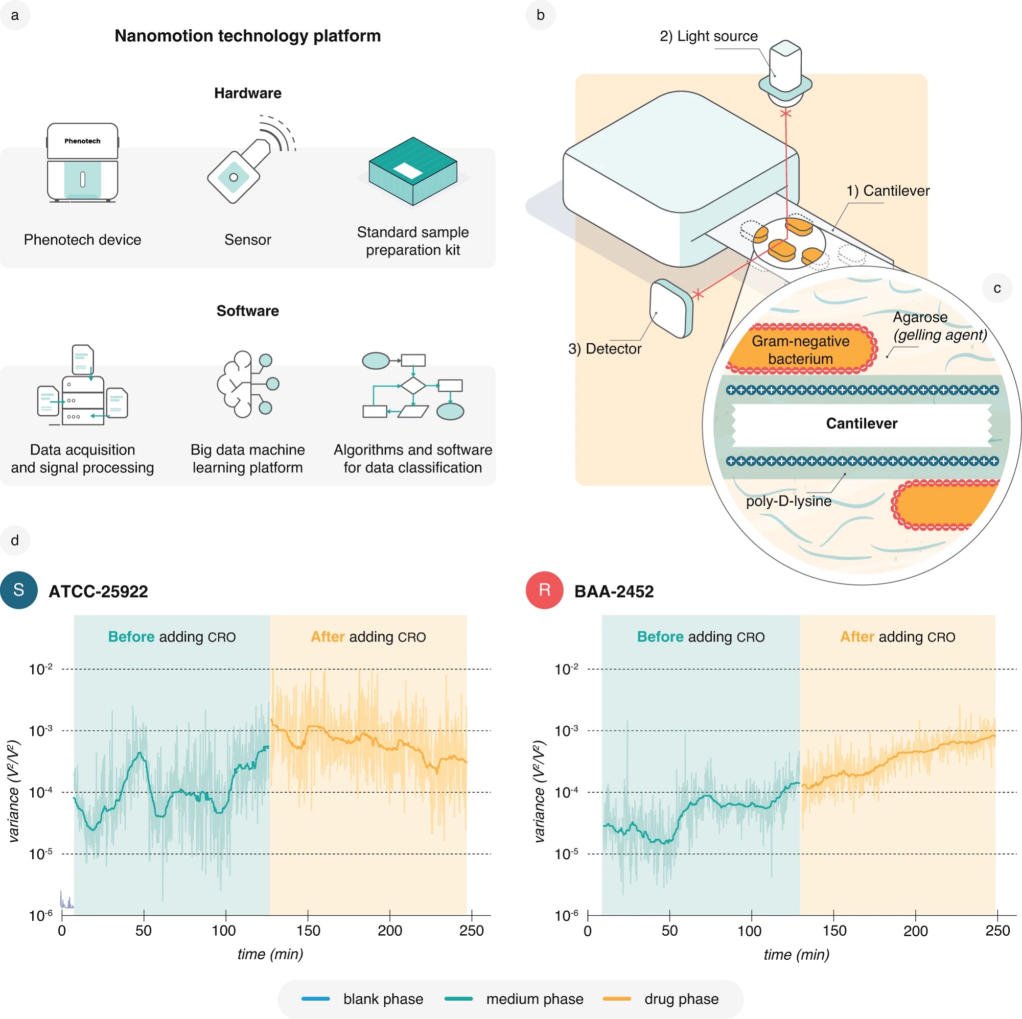
Accurate and rapid antibiotic susceptibility testing using a machine learning assisted nanomotion technology platformWed Apr 24 2024
#Antimicrobialresistance ( #AMR) has become a significant threat to public health worldwide. *
#Nanomotion technology is based on #atomicforcemicroscopy ( #AFM) and has been proposed as potential means of circumventing these limitations by measuring bacterial viability and response to antibiotics in a growth-independent manner. *
Here, a functionalized #AFMcantilever oscillates in response to #bacterialvibrations. Conditions that alter bacterial vibrations, such as drug exposure, modulate AFM cantilever oscillations, and these changes can be detected, measured, and outputted using an optical read-out system. *
Nanomotion technology can distinguish the differing responses of resistant and susceptible bacteria to antibiotic treatment and has already been employed to detect antibiotic susceptibility for several different microorganisms. *
In the article “Accurate and rapid antibiotic susceptibility testing using a machine learning-assisted nanomotion technology platform” Alexander Sturm, et al. describe a rapid growth-independent phenotypic #antibioticsusceptibilitytests ( #AST) that uses a nanomotion technology platform to measure bacterial vibrations. *
Nanomotion-based AST strategies utilize technologies that are well-established in atomic-force microscopy (AFM). The nanomotion detection system described in the article is based on an AFM setup for cantilever-based optical deflection detection. *
However, in contrast to standard AFM devices, in this device the light source and the photodetector are placed below the AFM cantilever to facilitate the experimental workflow. A light beam, focused at the AFM cantilever end, originates in a superluminescent diode (SLED) module (wavelength: 650 mm, optical power: 2 mW), is reflected, and reaches a four-sectional position-sensitive photodetector that is a part of a custom-made precision preamplifier. *
The flexural deflection of the AFM cantilever is transformed into an electrical signal, which is further processed by a custom-made dedicated electronic module and recorded using a data acquisition card. The device is controlled using a dedicated AST software. *
The custom-made tipless AFM probes used for the described experiments are quartz-like tipless cantilevers with a gold coating acting as a mirror for the light beam (NANOSENSORS™ uniqprobe SD-qp-CONT-TL, typical spring constant: 0.1 N/m, AFM cantilever length × width × thickness: 130 × 40 × 0.75 µm, typical resonant frequency in air: 32 kHz from the NANOSENSORS Special Developments List). *
During an AST experiment, bacterial #nanoscale movements actuate the AFM cantilever to deflect in specific frequencies and amplitudes. *
The study shows the potential of this nanomotion platform for future bacterial phenotype delineation. *
Please have a look at the NANOSENSORS blog for the full citation and a direct link to the full article.
https://www.nanosensors.com/blog/accurate-and-rapid-antibiotic-susceptibility-testing-using-a-machine-learning-assisted-nanomotion-technology-platform/
https://www.nanosensors.com/blog/accurate-and-rapid-antibiotic-susceptibility-testing-using-a-machine-learning-assisted-nanomotion-technology-platform/


Our ElectriTap300-G AFM probes have been used for piezoresponse force microscopy characterization of the MESO nanodeviceMon Apr 22 2024
“In conclusion, we have shown voltage-based writing and reading of magnetic states in a CoFe nanostructured element coupled with multiferroic BiFeO3, representing the proof-of-principle for the MESO logic concept… [T]hese results provide a key step forward toward voltage-control of magnetization in nanoscale magnets, essential for future low-power spin-based logic and memory devices.”
Our ElectriTap300-G AFM probes have been used for piezoresponse force microscopy characterization of the MESO nanodevice.


In Focus: Resist Recess Depth Monitoring of Narrow TrenchesMon Apr 22 2024
- Experimental setup:
Samples: Resist recess trenches on product wafers. Trenches were filled with resist and then etched back.
Tool: Park NX-Wafer operated in fully automated recipe mode, Park Systems
AFM probe: EBD4-200A, nanotools - Extracted feature parameters:
Resist recess trench depth - Key findings:
Single AFM tool (200 nm narrow, 1035 nm deep trenches)
0.6 nm < σ < 1.4 nm: 10-times dynamic repeatability of 5 dies
Accuracy: dimensional verification by cross sections in SEM
Measurement time: few seconds/site + 60 seconds for sample positioning
2 AFM tools: Fab to fab matching (480 nm deep trenches)
< 5 nm offset: 3 runs of 9-point recipe running the same wafer in 2 different fabs

High-Performance and Lithography-Free Au/WS2/Ag Vertical Schottky Junction Solar CellsThu Apr 18 2024
Transition metal dichalcogenide (TMD) semiconductors (SCs) exhibit intriguing optical, electrical, and mechanical properties. *
Due to their extraordinarily large optical absorption coefficients, #transitionmetaldichalcogenides (TMDs) are gaining more and more attention for #photovoltaicapplications. Improving the device performance of a #TMDsolarcell requires an optimal device architecture and reliable fabrication processes. *
Improving the device performance of a TMD solar cell requires an optimal device architecture and reliable fabrication processes. *
In the article “High-Performance and Lithography-Free Au/WS2/Ag Vertical Schottky Junction Solar Cells” Anh Thi Nguyen, Jun Wang, Eunseo Cho, Seoyoung Lim, Soyeong Kwon, Jungeun Song, Keya Zhou and Dong-Wook Kim describe how they fabricated Au/WS2/Ag vertical Schottky diodes and investigated their photovoltaic characteristics. *
Metal/WS2-multilayer/metal heterojunctions were fabricated using lithography-free processes. 20 nm thick #WS2 flakes were exfoliated on template-stripped Ag bottom electrodes, and then 10 nm thick Au top electrodes with a diameter of 2 µm were evaporated on the WS2 surface using holey carbon films as shadow masks. *
#CurrentsensingAtomicForceMicroscope measurements revealed that the Au/WS2/Ag devices exhibit prominent rectifying characteristics, indicating the formation of #Schottkydiodes. *
The #surfacemorphology and the local current of the samples were simultaneously measured using a current-sensing atomic force microscopy ( #cAFM) system in a #glovebox. For transport measurements with nanoscopic spatial resolution, a wear-resistant highly doped NANOSENSORS™ PointProbe® Plus conductive diamond-coated #AFMtip with a typical spring constant of 0.5 N m and a typical resonance frequency of 20 kHz (CDT-CONTR AFM probe type) was employed. *
The power conversion efficiency of the #Schottkyjunction was as high as 5.0%, when illuminated by a light-emitting diode with a peak wavelength of 625 nm and a power density of 2.5 mW cm−2. These devices also possess broadband and incident-angle-insensitive absorption capability due to the very large refractive indices and extremely small thickness of the WS2 flakes. The simple fabrication procedures proposed in the article by Anh Thi Nguyen et al. demonstrate high-performance and high-yield TMD photovoltaic devices.*
Please have a look at the NANOSENSORS blog for the full citation and a direct link to the full article.
Electrochemical detection of quinone reduced by Complex I Complex II and Complex III in full mitochondrial membranesMon Apr 15 2024
Electrochemical detection of quinone reduced by Complex I Complex II and Complex III in full mitochondrial membranes
In the last decades enormous advances have been made in characterizing the atomic and molecular structure of respiratory chain supercomplexes. * However, it still remains a challenge to stitch this refined spatial atomistic description with functional information provided by biochemical studies of isolated protein material. Development of functional assays that detect respiratory chain complexes in their native membrane environment contribute to address the open questions related to the role played by their association and interactions. * In the article “Electrochemical detection of quinone reduced by Complex I Complex II and Complex III in full mitochondrial membranes” Daniel G. Cava, Julia […]
#AFMCharacterization, #AFMProbes, #AFMTopographyImaging, #AFMカンチレバー, #AFMプローブ, #AFM探针, #AtomicForceMicroscopy, #Biochemistry, #BiologyAFMProbes, #CellularBiochemistry, #ElectrochemicalDetection, #Electrochemistry, #Mitochondria, #MitochondrialMembrane, #MitochondrialMembranes, #PNPDB, #PyrexNitrideAFMProbes, #Quinone, #RespiratoryChainProteins, #SiliconNitrideAFMProbes, #TetheredFloatingBilayers, #原子力显微镜, #原子力显微镜探针, #扫描探针显微镜探针

Graphene removal by water-assisted focused electron-beam-induced etching – unveiling the dose and the dwell time impact on the etch profile and topographical changes in SiO2 substratesWed Mar 27 2024
#Graphene is one of the most extensively studied #2Dmaterials, exhibiting extraordinary mechanical and electronic properties. *
Although many years have passed since its discovery, manipulating single graphene layers is still challenging using standard resist-based lithography techniques. *
Recently, it has been shown that it is possible to etch graphene directly in water-assisted processes using the so-called #FocusedElectronBeamInducedEtching ( #FEBIE), with a spatial resolution of ten nanometers. *
#Nanopatterning graphene with such a method in one single step and without using a physical mask or resist is a very appealing approach. *
In the article “Graphene removal by water-assisted focused electron-beam-induced etching – unveiling the dose and dwell time impact on the etch profile and topographical changes in SiO2 substrates “ Aleksandra Szkudlarek, Jan M. Michalik, Inés Serrano-Esparza, Zdeněk Nováček, Veronika Novotná, Piotr Ozga, Czesław Kapusta and José María De Teresa describe how, during the process, on top of #graphenenanopatterning, they found significant morphological changes induced in the SiO2 substrate even at low electron dose values (<8 nC/μm2). *
They demonstrate that #grapheneetching and topographical changes in SiO2 substrates can be controlled via electron beam parameters such as dwell time and dose. *
The feasibility of water-assisted FEBIE, available on scanning electron microscopes operating in low-vacuum mode, makes the method very promising for prototyping various optical/electronic devices based on graphene. *
In their article, Aleksandra Szkudlarek et al. show that with certain precautions water-assisted FEBIE can be applied for such a nanopatterning process. *
The experimental data obtained with scanning Raman spectroscopy, correlative probe and electron microscopy, and in situ AFM measurements provide a comprehensive image of FEBIE etch profiles. *
Precise surface analysis of etched structures can be performed by #atomicforcemicroscopy. The authors used an #AFM setup capable of integrating into a scanning electron microscope (SEM). They used the #CorrelativeProbeandElectronMicroscopy ( #CPEM) technology for simultaneous acquisition of #AFM and #SEM signals, enabling an efficient and complex surface analysis.
The #AFMinSEM approach allowed for in situ analysis.
Thus, the graphene could be modified and immediately measured by AFM without changing the environment. *
The analysis was performed by using the tapping mode and the NANOSENSORS™ Akiyama probe (a tuning fork based self-sensing and self-actuating #AFMprobe, A-Probe)
Please have a look at the NANOSENSORS blog for the full citation and a direct link to the full article.

Variations of Collagen Properties Following Accumulation of Advanced Glycation End-productsMon Mar 25 2024
- Title: Modulation of the biophysical and biochemical properties of collagen by glycation for tissue engineering applications
- DOI: 10.1016/j.actbio.2022.11.033
- Authors: Mina Vaez, Meisam Asgari, Liisa Hirvonen, Gorkem Bakir, Emilie Khattignavong, Maya Ezzo, Sebastian Aguayo, Christina M. Schuh, Kathleen Gough, Laurent Bozec
- Publication: Acta Biomaterialia
- Publisher: Elsevier
- Date: 1 January 2023


NanoAndMore Japan is exhibiting at the 71st Spring Academic Conference of the Japan Society of Applied PhysicsFri Mar 22 2024
NanoAndMore Japan https://www.nanoandmore.jp/ is exhibiting at the 71st Spring Academic Conference of the Japan Society of Applied Physics
Please feel free to drop by our booth No. E145 to learn more about the many different #AFMprobe types we offer from many different manufacturers and feel free to discuss your #atomicforcemicroscopy applications with us.
22~25 March, 2024
Setagaya Campus, Tokyo City University https://meeting.jsap.or.jp/english
@JSAPmeeting @JSAP_official @JSAP_EXPO
NanoAndMoreジャパンは日本応用物理学会 春季学術講演会に出展しています。Thu Mar 21 2024
@NanoAndMoreジャパン https://www.nanoandmore.jp/ は日本応用物理学会 春季学術講演会に出展しています。お気軽にお立ち寄りください。Booth No.E145
応用物理学会 EXPO Spring 2024
Manipulating hyperbolic transient plasmons in a layered semiconductorTue Mar 19 2024
Manipulating hyperbolic transient plasmons in a layered semiconductor
Anisotropic materials with oppositely signed dielectric tensors support hyperbolic polaritons, displaying enhanced electromagnetic localization and directional energy flow. * However, the most reported hyperbolic phonon polaritons are difficult to apply for active electro-optical modulations and optoelectronic devices. * In the nature communications letter “Manipulating hyperbolic transient plasmons in a layered semiconductor”, Rao Fu, Yusong Qu, Mengfei Xue, Xinghui Liu, Shengyao Chen, Yongqian Zhao, Runkun Chen, Boxuan Li, Hongming Weng, Qian Liu, Qing Dai and Jianing Chen report a dynamic topological plasmonic dispersion transition in black phosphorus (BP) via photo-induced carrier injection, i.e., transforming the iso-frequency contour from a pristine ellipsoid […]
#2DMaterials, #AFMProbes, #AFMカンチレバー, #AFMプローブ, #AFM探针, #AnisotropicMaterials, #ArrowAFMProbe, #ArrowAFMTip, #ArrowNCPt, #BlackPhosphorus, #ConductiveAFMTip, #LayeredSemiconductor, #MaterialsResearch, #MaterialsScience, #Nanophotonics, #NanophotonicsAndPlasmonics, #Nanoplasmonics, #Nanoscopy, #OptoelectronicApplications, #Optoelectronics, #Plasmonics, #Polaritons, #SSNOM, #ScatteringTypeScanningNearFieldOpticalMicroscopy, #SubWavelengthOptics, #TwoDimensionalMaterials, #UltrafastNanoscopy, #UltrafastPhotonics, #散乱型走査型近接場光学顕微鏡, #散射型扫描近场光学显微镜, #超快纳米显微镜, #超高速ナノスコピー

Mitochondrial‐derived vesicles retain membrane potential and contain a functional ATP synthaseFri Mar 15 2024
Vesicular transport is a means of communication. *
While cells can communicate with each other via secretion of extracellular vesicles, less is known regarding organelle‐to organelle communication, particularly in the case of #mitochondria . *
Mitochondria are responsible for the production of energy and for essential metabolic pathways in the cell, as well as fundamental processes such as apoptosis and aging. *
In the article “Mitochondrial‐derived vesicles retain membrane potential and contain a functional ATP synthase” Reut Hazan (Ben‐Menachem), Dvora Lintzer, Tamar Ziv, Koyeli Das, Irit Rosenhek‐Goldian, Ziv Porat, Hila Ben Ami Pilo, Sharon Karniely, Ann Saada, Neta Regev‐Rudzki and Orphry Pines show that functional mitochondria isolated from Saccharomyces cerevisiae release vesicles, independent of the fission machinery. *
They isolate these #mitochondrialderivedvesicles (MDVs) and find that they are relatively uniform in size, of about 100 nm, and carry selective protein cargo enriched for ATP synthase subunits. *
Imaging analyses of mitochondrial‐derived #vesicles by #atomicforcemicroscopy ( #AFM ) and transmission electron microscopy (TEM), verified that these vesicles are within a range of 50 to 200 nm diameter. *
Images were captured with atomic force microscopy using NANOSENSORS uniqprobe qp-BioAC-CI (CB2 or CB1 ) #AFMprobes. The qp-BioAC-CI AFM probes with their rounded AFM tips (typical AFM tip radius 30nm) on three soft #AFMcantilevers ( typical spring constant CB1: 0.3 N/m , typical spring constant CB2: 0.1 N/m, typical spring constant CB3: 0.06 N/m ) are especially designed for #cellimaging. *
Please find the full citation and a direct link to the full article in our NANOSENSORS blog

Studying the cation dependence of CO2 reduction intermediates at Cu by in situ VSFG spectroscopyFri Mar 08 2024
Studying the cation dependence of CO2 reduction intermediates at Cu by in situ VSFG spectroscopy
The nature of the electrolyte cation is known to have a significant impact on electrochemical reduction of CO2 at catalyst|electrolyte interfaces. An understanding of the underlying mechanism responsible for catalytic enhancement as the alkali metal cation group is descended is key to guide catalyst development. * In the article “Studying the cation dependence of CO2 reduction intermediates at Cu by in situ VSFG spectroscopy” Liam C. Banerji, Hansaem Jang, Adrian M. Gardner and Alexander J. Cowan use in situ vibrational sum frequency generation (VSFG) spectroscopy to monitor changes in the binding modes of the CO intermediate at the electrochemical interface […]
#AFMCharacterization, #AFMProbes, #AfmTips, #AFMカンチレバー, #AFMプローブ, #AFM探针, #AtomicForceMicroscopy, #CatalystDevelopment, #CatalyticEnhancement, #Characterization, #Chemistry, #CObridge, #ContactMode, #CONTR, #ElectrochemicalCO2Reduction, #ElectrolyteInterfaces, #Morphology, #Pointprobe, #PointprobeCONTR, #SurfaceMorphology, #原子力显微镜, #原子力显微镜探针

Correlation between the Dimensions and Piezoelectric Properties of ZnO Nanowires Grown by PLI-MOCVD with Different Flow RatesMon Mar 04 2024
#Zincoxidenanowires (ZnO NWs) have gained considerable attention in the field of #piezoelectricity in the past two decades. However, the impact of growth-process conditions on their dimensions and polarity, as well as the piezoelectric properties, has not been fully explored, specifically when using pulsed-liquid injection metal–organic chemical vapor deposition (PLI-MOCVD). *
For the article “Correlation between the Dimensions and Piezoelectric Properties of ZnO Nanowires Grown by PLI-MOCVD with Different Flow Rates” Quang Chieu Bui, Vincent Consonni, Carmen Jiménez, Hervé Roussel, Xavier Mescot, Bassem Salem and Gustavo Ardila investigated the influence of the O2 gas and DEZn solution flow rates on the formation process of ZnO NWs and their related piezoelectric properties. *
While the length and diameter of ZnO NWs were varied by adjusting the flow-rate conditions through different growth regimes limited either by the O2 gas or DEZn reactants, their polarity was consistently Zn-polar, as revealed by #piezoresponseforcemicroscopy ( #PFM ) .*
Moreover, the piezoelectric coefficient of ZnO NWs exhibits a strong correlation with their length and diameter. The highest mean piezoelectric coefficient of 3.7 pm/V was measured on the ZnO NW array with the length above 800 nm and the diameter below 65 nm. These results demonstrate the ability of the PLI-MOCVD system to modify the dimensions of ZnO NWs, as well as their piezoelectric properties.*
NANOSENSORS™ conductive and wear-resistant Platinum-Silicide #AFMprobes of the PtSi-NCH type with a high spring constant (typical value 42 N/m) were used to mitigate the interference of the electrostatic effect during the measurements.*
In the DataCube PFM mode, the #AFMtip was systematically brought into contact with the sample at a determined position, subsequently held in 60 milliseconds for the piezoelectric measurement, and then retracted before proceeding to the next position. This sequential approach and retraction of the AFM tip was employed to avoid tip dragging during the scanning process, which could bend the NWs and cause a contact failure between the AFM tip and the sample. When the AFM tip was in contact with the sample, an AC voltage of 5 V amplitude and 15 kHz frequency of AC voltage was applied across the top and bottom of the sample through the tip and chuck of the AFM system. Due to the piezoelectric properties, the ZnO NWs were deformed in response to the AC voltage. This deformation was measured by the AFM tip to obtain the piezoelectric response amplitude and phase signals. The piezoelectric response amplitude is proportional to the piezoelectric coefficient, while the piezoelectric response phase identifies the polarity of ZnO NWs. Thanks to the small radius of the AFM tip, the piezoelectric response of each individual NW can be measured. By scanning the AFM tip across a 1 × 1 µm2 area, the piezoelectric response of the NWs in the array was mapped. For each sample, the piezoresponse amplitude values were extracted from the piezoresponse amplitude map, and the mean piezoresponse amplitude was evaluated to study the piezoelectric amplitude behavior of ZnO NWs grown at different flow rates.*
Please have a look at the NANOSENSORS blog for the full citation and a direct link to the full article.
Structural and optical variation of pseudoisocyanine aggregates nucleated on DNA substratesTue Feb 27 2024
Structural and optical variation of pseudoisocyanine aggregates nucleated on DNA substrates
The ability to maximize the range of exciton transport while minimizing energy loss has significant implications for the design of future nanoscale light harvesting, optoelectronic, and sensing applications. * One method of achieving this would be to densely pack dyes into strongly coupled aggregates such that excitations can be coherently delocalized through the partial or full length of the aggregate. * Coherently coupled aggregates enable exciton migration over discreet spatial distances with near unitary quantum efficiency. As a result, controlled dye aggregation has long been studied by chemists as a method of tuning the photonic and physical properties of the […]
#AFMCharacterization, #AFMInLiquid, #BiophysicalCharacterization, #Characterization, #CircularDichroism, #DNANanostructures, #DNAScaffolds, #DyeAggregates, #EnergyTransfer, #FluorescenceSpectroscopy, #HighSpeedScanning, #HighSpeedAtomicForceMicroscopy, #Nanostructures, #Pseudoisocyanine, #PseudoisocyanineDye, #UltraHighFrequencyAFMCantilevers, #UltraHighFrequencyAFMProbes, #UltraHighFrequencyCantilevers, #UltraShortAFMCantilevers, #UltrafastScanning, #USC, #USCF03K03, #UVVisSpectroscopy, #VideoRateAFM, #VisualizationOfDNABasedPICAggregates, #VisualizationOfDNABasedPseudoisocyanineAggregates, #高速AFM, #高速AFMカンチレバー, #高速AFMプローブ, #高速AFM探针, #高速原子力显微镜, #高速原子力显微镜探针

Quantitative wear evaluation of tips based on sharp structuresMon Feb 26 2024
“This paper demonstrates the utility of sharp structures in assessing the topography of AFM tips and delves into the effects of scanning parameters on tip wear. A method employing BudgetSensors™ Tipcheck samples has been introduced to determine the shape and structure of AFM tips accurately. Based on its distinct features, the tip morphology can be non-destructively assessed using the AFM imaging mode. This offers a compelling alternative to the conventional SEM detection method. ”

Model of a graphite electrodeFri Feb 23 2024
Interface analysis between a model for the graphite electrode and solvent for electrolytes of lithium-ion batteries. An example of the interface observation between highly oriented pyrolytic graphite (HOPG) as a model for graphite electrodes and tetraglyme, which has been studied as a solvent of electrolytes for lithium ion batteries. The AFM cantilever oscillation frequency and amplitude during the experiments were 92 kHz and 0.3 nm, respectively. The temperature was maintained at 298 K under an argon atmosphere throughout the experiment to prevent the dissolution of contaminants from the air, which could affect the interface structure. The topographic image revealed an ordered structure at Δf = 1000 Hz, obtained with tetraglyme adsorbed on an HOPG surface.
Scanned with a NANOSENSORS PointProbe® Plus PPP-NCHAuD AFM probe in FM mode.
Image courtesy of Dr. Taketoshi Minato, Institute for Molecular Science, National Institutes of Natural Sciences, Okazaki, Japan.

AFM Viscoelastic Quantification Over 5 Orders of Magnitude Frequency RangeThu Feb 22 2024
Discover how nanotools biosphere™ with 2µm radius are applied to quantify the nanoscale loss tangent, storage modulus, and loss modulus of polymeric materials.
- Title: Nanoscale rheology: Dynamic Mechanical Analysis over a broad and continuous frequency range using Photothermal Actuation Atomic Force Microscopy
DOI: 10.1021/acs.macromol.3c02052 - Authors: Alba R. Piacenti, Casey Adam, Nicholas Hawkins, Ryan Wagner, Jacob Seifert, Yukinori Taniguchi, Roger Proksch, and Sonia Contera
- Publication: Macromolecules
- Publisher: American Chemical Society
- Date: January 16 2024
Highlights


AFM Probe Focus


best of the best
qp-HBC
uniqprobe™ - HeartBeat Cantilever for ScanAsyst®** and Peak Force Tapping™**
Coating:
Reflective Aluminum
Tip Shape: Circular symmetric
Tip Shape: Circular symmetric
AFM Cantilever:
F
60 kHz
C
0.5 N/m
L
115 µm
ATEC-NC
Tapping Mode AFM Probe with REAL Tip Visibility
Coating:
none
Tip Shape: Visible
Tip Shape: Visible
AFM Cantilever:
F
335 kHz
C
45 N/m
L
160 µm
TESPA
Standard Tapping Mode AFM Probe
Coating:
Reflective Aluminum
Tip Shape: Standard
Tip Shape: Standard
AFM Cantilever:
F
320 kHz
C
42 N/m
L
125 µm
OTESPA
Standard Tapping Mode AFM Probe with AFM Tip at the Very End of the AFM Cantilever
Coating:
Reflective Aluminum
Tip Shape: Optimized Positioning
Tip Shape: Optimized Positioning
AFM Cantilever:
F
300 kHz
C
26 N/m
L
160 µm